

Semiconductor memory equipped with row address decoder having reduced signal propagation delay time
a technology of signal propagation delay and memory, which is applied in the field of semiconductor memory, can solve the problems of affecting the high-speed operation of semiconductor memory, increasing the access time of semiconductor memory, and increasing the cost compared with the configuration of fig
- Summary
- Abstract
- Description
- Claims
- Application Information
AI Technical Summary
Problems solved by technology
Method used
Image

Examples
first embodiment
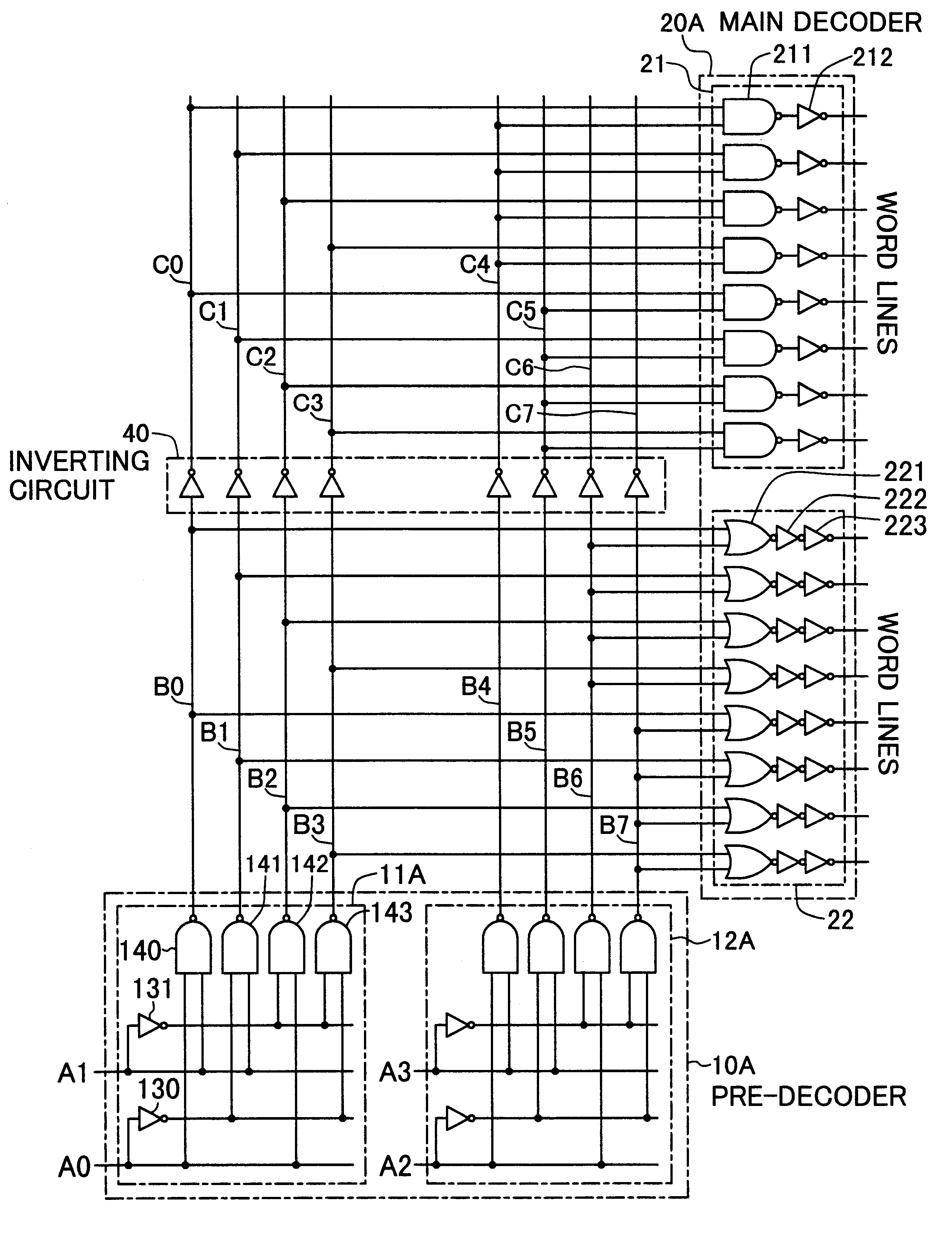
FIG. 1 shows a 4-bit row address decoder circuit of a first embodiment according to the present invention.
This circuit includes a pre-decoder 10A, a main decoder 20A, and an inverting circuit 40.
The pre-decoder 10A includes a decoder 11A for lower 2 bits A1 and A2 of a row address, and a decoder 12A for higher 2 bits A3 and A4 of the row address.
In the decoder 11A, there are combined one of a signal A0 and an inverted signal thereof by an inverter 130 and one of a signal A1 and an inverted signal thereof by an inverter 131, and all the combinations thereof are provided to individual NAND gates 140 to 143. The outputs of the NAND gates 140 to 143 are connected to lines B0 to B3, respectively. With such a configuration, one of the lines B3 to B0 is low according to a value of the lower 2 row address bits A1 and A0 while the others of the lines B3 to B0 are high.
The decoder 12A has the same configuration as the decoder 11A, receives the higher 2 row address bits A3 and A2, and the four...
second embodiment
FIG. 6 is a layout sketch of circuit blocks in a semiconductor chip of a second embodiment according to the present invention.
In this chip, on one side of an address control circuit 30B and data I / O control circuits 33A and 34A, there are disposed the memory cell arrays MC1 to MC4, the inverting circuit 40, the minor sense amplifier circuits 50 and 51 and the main decoders 21 and 22, while on the other side thereof, there are disposed memory cell arrays MC5 to MC8, an inverting circuit 41, minor sense amplifier circuits 52 and 53 and main decoders 23 and 24, wherein corresponding constituents on both sides are arranged in symmetry. The address control circuit 30B, and the data I / O control circuits 33A and 34A are shared by the circuits on both sides.
With such a configuration, the chip area can be smaller than the case where double the circuit of FIG. 17 are arranged adjacent to each other in parallel.
third embodiment
FIG. 7 shows a 4-bit row address decoder circuit of a third embodiment according to the present invention.
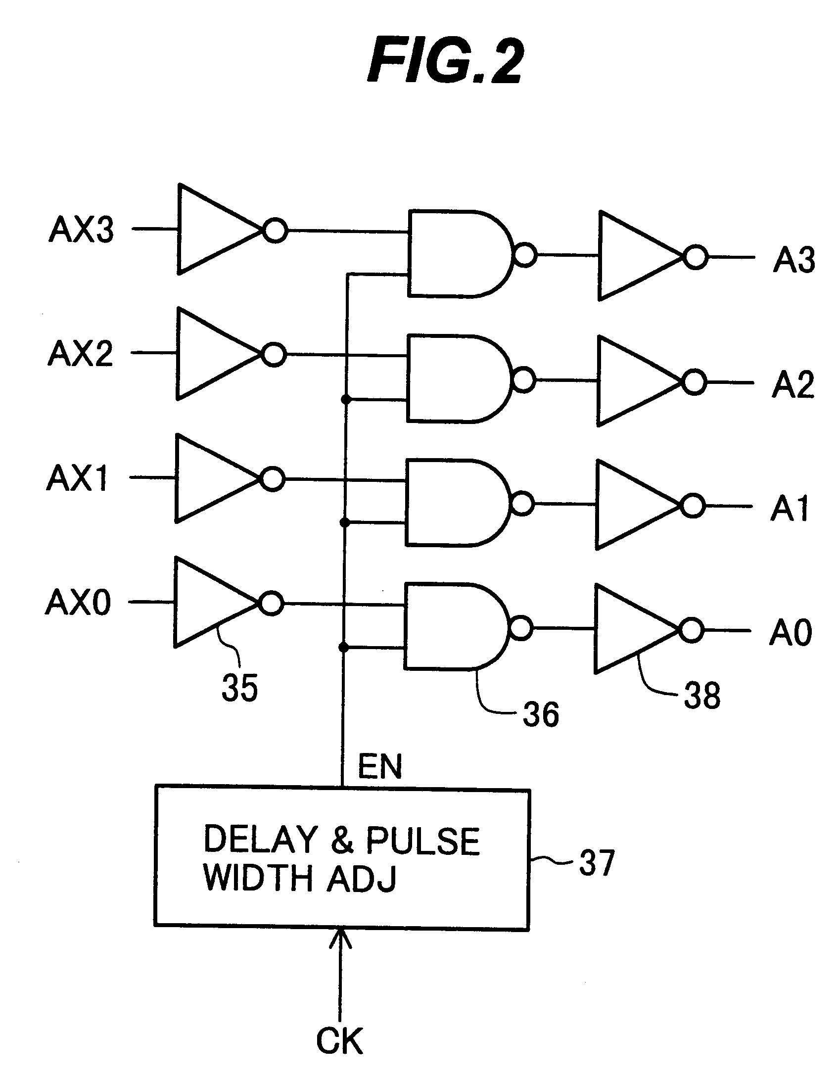
In this circuit, the enable signal EN is provided through an inverter 42 to the NOR gates of a main decoder 22A, and the output of the inverter 42 is provided through an inverter 43 to the AND gates of a main decoder 21A. With such a configuration, the output of the main decoder 20B consisting of the main decoders 21A and 22A is effective only while the enable signal EN is high, therefore a memory cell activation time is reduced with the result that power consumption decreases. Note that the enable signal EN is generated by providing an external clock CK to the delaying and pulse width adjusting circuit 37 as shown in FIG. 2.
The inverters 42 and 43 are disposed adjacent to the pre-decoder 10A and the inverting circuit 40, respectively. The inverter 43 is used for not only corresponding to the different logic polarities of the inputs of the main decoders 21A and 22A but also decr...
PUM
 Abstract
Description
Claims
Application Information