Method of producing semiconductor device with heat dissipation metal layer and metal projections

a technology of heat dissipation metal and metal projection, which is applied in the direction of solid-state devices, basic electric elements, manufacturing tools, etc., can solve the problems of difficult reduction of production costs, poor appearance of the cut portion, and limit the improvement of production yield

Inactive Publication Date: 2001-06-12
MITSUBISHI ELECTRIC CORP
View PDF11 Cites 26 Cited by
  • Summary
  • Abstract
  • Description
  • Claims
  • Application Information

AI Technical Summary

Problems solved by technology

Thus there has been a limitation to the improvement in the production yield and it has been difficult to reduce the production costs due to the complicated producing process.
While the use of the two metal layers has an advantage that bending and cracking of the metal layer can be reduced during the production steps, the thick film may cause poor appearance of the cut portion and the generation of devices having poor appearance has been impeding the improvement in the production yield.
There has also been such a problem that the first metal layer and the second metal layer peel off each other when the second metal layer is formed in an electrolytic plating process.
When the thickness is less than 500 .ANG., the film is difficult to function as an anti-oxidation film for the plated feeder layer.
Also because the laser beam of excessively high output cuts off the expand sheet bonded onto the bottom surface of the PHS layer which should not be cut.

Method used


Image

  • Method of producing semiconductor device with heat dissipation metal layer and metal projections
  • Method of producing semiconductor device with heat dissipation metal layer and metal projections
  • Method of producing semiconductor device with heat dissipation metal layer and metal projections

Examples


first embodiment

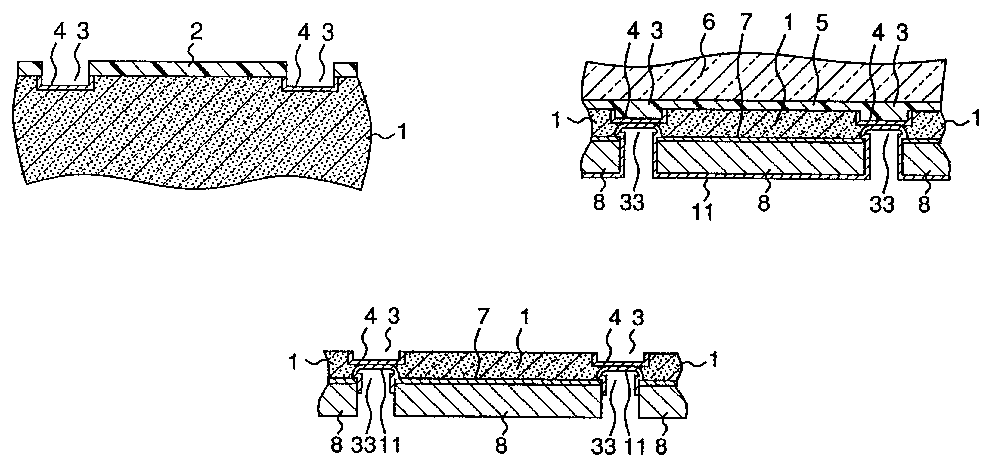
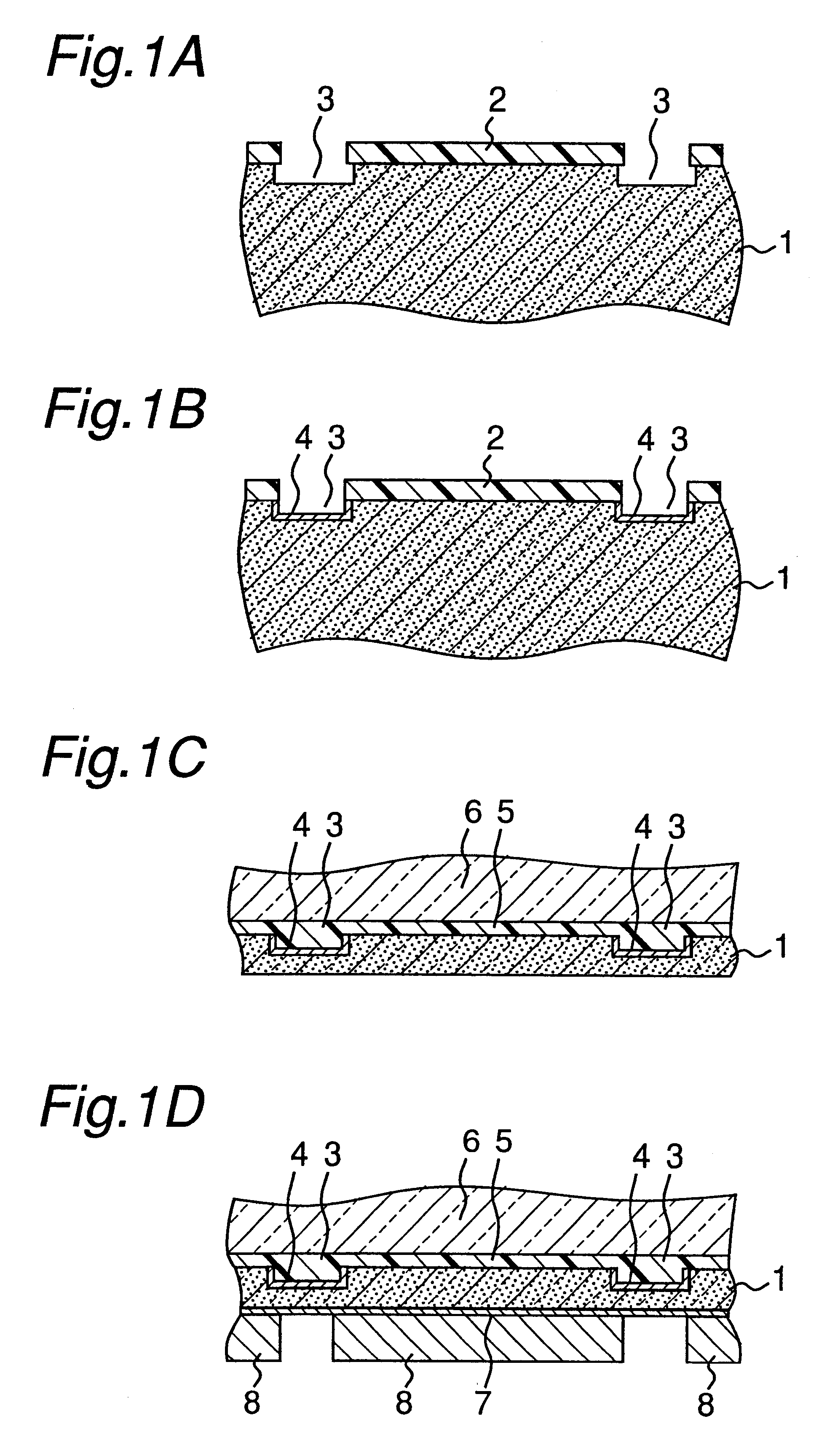
A method of producing semiconductor devices according to the present invention will now be described below with reference to FIGS. 1A through FIG. 1L. Reference numerals identical with those used in FIGS. 3A through FIG. 3k denote the same or corresponding components.

According to the first embodiment of the method of present invention, a first separation groove is formed on the surface of a GaAs substrate 1 having semiconductor elements formed thereon in an etching step using a photoresist layer 2 as a mask (FIG. 1A). Then, a first metal layer 4 is formed in the first separation groove by vapor deposition, sputtering, non-electrolytic plating method, or the like (FIG. 1B), in the steps similar to those of the prior art. The first metal layer 4 is preferably a Ni alloy layer selected from Ni--P, Ni--B and Ni--B--W.

While the first metal layer 4 has a reflectivity for YAG laser light used in laser cutting preferably less than about 80%, a more preferable value of reflectivity within 8%...

embodiment 2

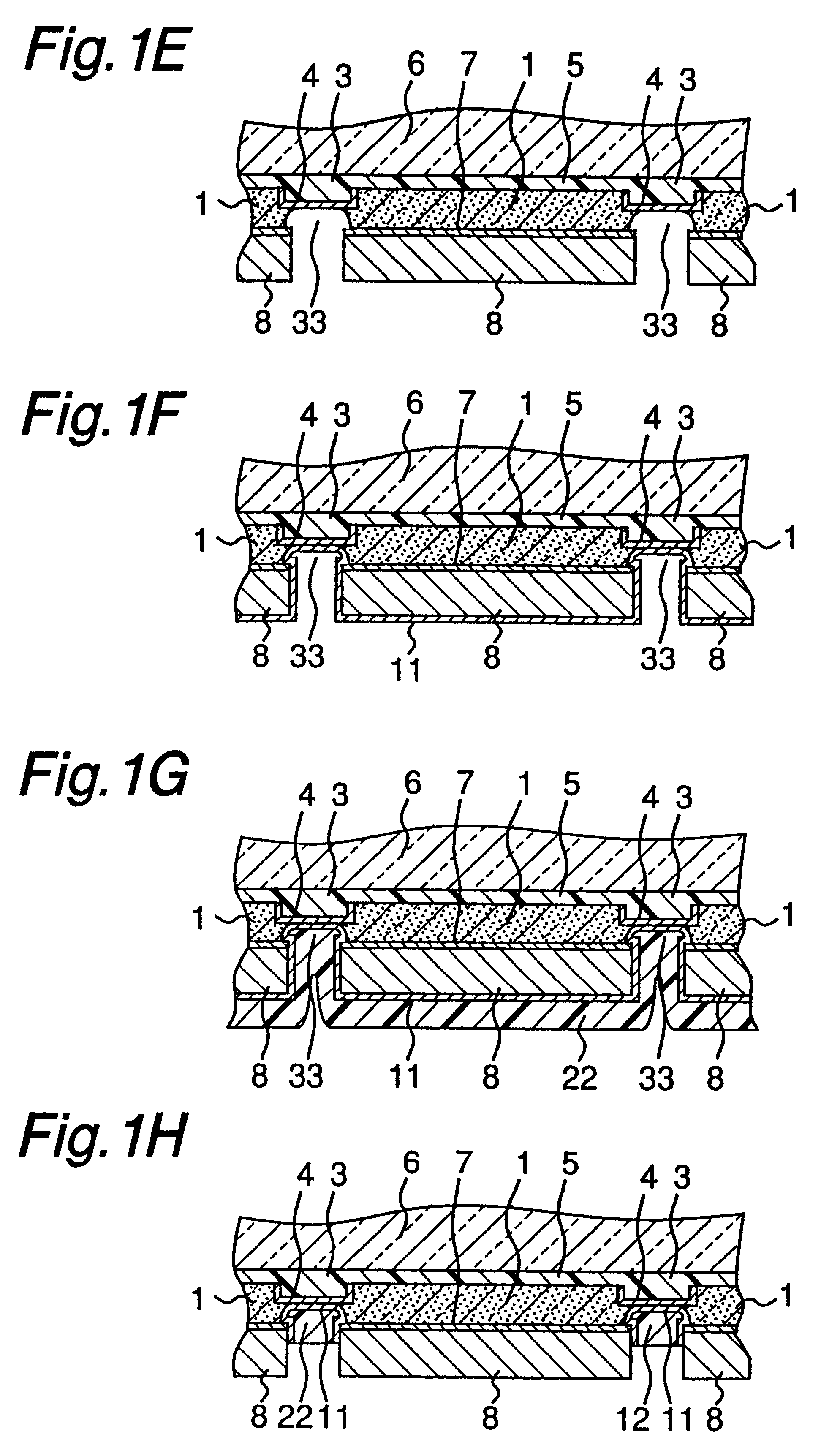
A second embodiment of the present invention will now be described below with reference to FIGS. 2A-2C. Reference numerals in the drawing identical with those used in FIGS. 1A through FIG. 1L denote the same or corresponding components.

First the processes shown in FIGS. 1A through FIG. 1F of the first embodiment are carried out to form the second metal layer 11 made of Ni or the like on the surface of the PHS layer 8 and the surface (entire surface on the back side) of the second separation groove 33.

Subsequently, a thin Ti film having a thickness of about 0.05 .mu.m and a thin Au film having a thickness of about 0.2 to 0.3 .mu.m are formed successively on the entire surface, covering the second metal layer 11, by sputtering or vapor deposition, thereby making a Ti / Au layer 13. At this time, because the Ti / Au layer 13 is formed on the side face of the PHS layer 8 as well, wettability of the back surface and side faces of the PHS layer 8 with the AuSn solder can be improved during di...


PUM

PropertyMeasurementUnit
reflectivityaaaaaaaaaa
thicknessaaaaaaaaaa
thicknessaaaaaaaaaa

Abstract

A method of producing a semiconductor device having a heat dissipating metal layer wherein the number of patterning steps is reduced, laser dicing produces a better profile, and first and second metal layers are prevented from separating from each other, and a semiconductor device produced by the method. The number of patterning steps is reduced by employing a flat exposure step for photoresist with mask alignment. A better appearance is obtained by forming the metal layers which connect the semiconductor devices with each other from a first metal layer having a lower melting point and a second metal layer having a higher melting point and severing the first metal layer and the second metal layer successively, from the first metal layer side. A second metal layer is prevented from peeling by preventing oxidation of the plated feeder layer through plating of the second metal layer.

Description

1. Field of the InventionThe present invention relates to a semiconductor device having a heat dissipation metal layer (PHS: Plated Heat Sink) provided on the back side thereof, and a method of producing the semiconductor device wherein devices are separated by laser cutting.2. Description of the Related ArtFIG. 3A through FIG. 3k show a method of producing a semiconductor device having a heat dissipation metal layer of the prior art disclosed in PCT application No. JP / 96 / 02758.According to such a method, a first separation groove 3 is formed by etching the surface of a GaAs substrate 1, on which semiconductor elements have been formed in advance, by using a photoresist layer 2 as a mask (FIG. 3A), then a first metal layer is formed in the first separation groove 3 by plating or another process (FIG. 3B).Then the GaAs substrate 1 is coated with a wax 5 and is bonded onto a carrier substrate 6 such as glass plate or sapphire plate, with the GaAs substrate 1 being polished on the back...

Claims


Application Information

Patent Timeline
Patent Type & Authority Patents(United States)
IPC IPC(8): H01L21/70H01L23/367H01L23/34H01L21/78B23K26/38B23K26/40H01L21/301H01L21/304
CPCH01L21/78H01L23/3677H01L2924/0002H01L2924/00
Inventor KOSAKI, KATSUYATAMAKI, MASAHIROMATSUOKA, HIROSHI
Owner MITSUBISHI ELECTRIC CORP
Why Eureka
Try Eureka