Grade for cast iron
a technology of grade and cast iron, applied in the direction of turning apparatus, magnetic recording, chemical vapor deposition coating, etc., can solve the problems of accelerated wear, unsatisfactory adhesion of ticn layer to underlying ticn layer,
- Summary
- Abstract
- Description
- Claims
- Application Information
AI Technical Summary
Benefits of technology
Problems solved by technology
Method used
Image
Examples
example 1
Two samples were made according to the prior art:
1) TiCN CVD layer, thickness 6 .mu.mm
Bonding layer
.alpha.+.kappa. alumina layer, thickness 6 .mu.m
(2) TiCN MTCVD layer, thickness 6 .mu.m
Bonding layer according to the prior art
.kappa. alumina layer, thickness 6 .mu.m
And two coatings according to the presently claimed invention
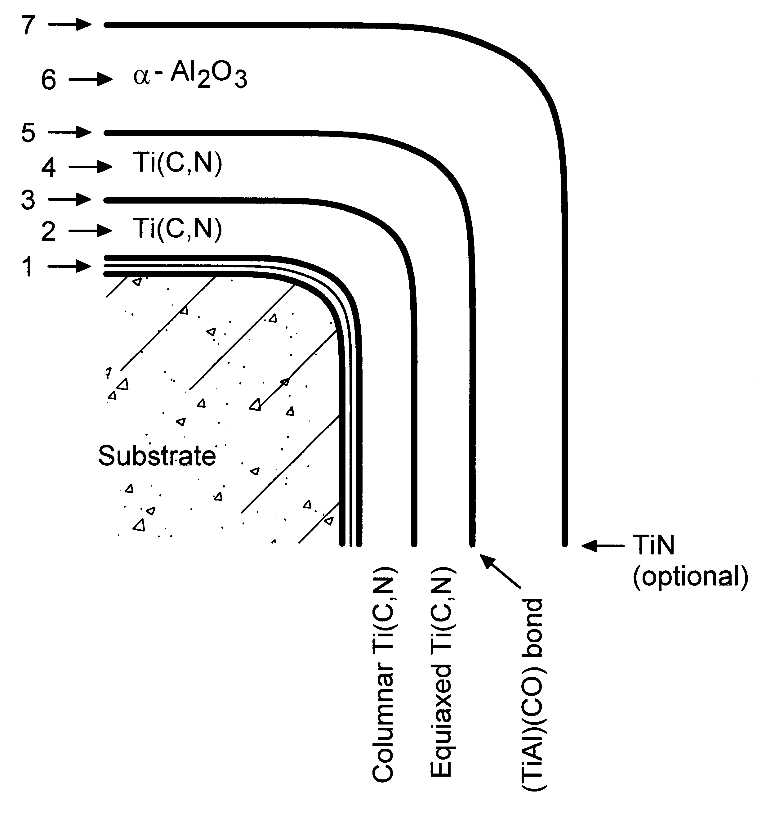
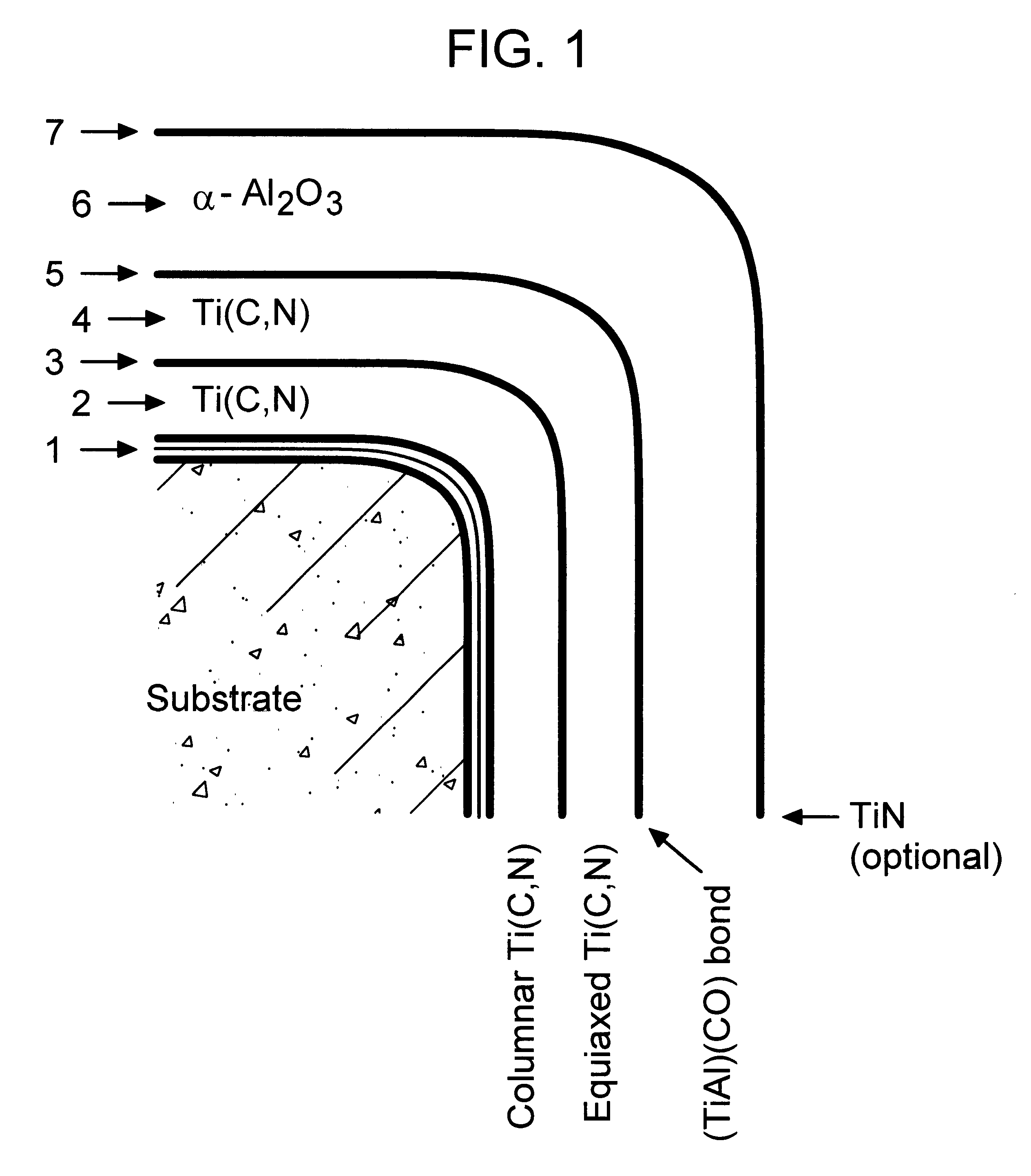
(3) A CVD bonding layer with epitaxy
TiCN MTCVD layer of columnar grains about 0.5 .mu.m width and 2.5 .mu.m length deposited using CH.sub.3 CN and CH.sub.4, thickness 4 .mu.m
TiCN CVD layer of equiaxed grains, about 0.5 .mu.m grain size, thickness 2 .mu.m
A bonding layer
.alpha.-Al.sub.2 O.sub.3 layer having a thickness of 6 .mu.m
A CVD bonding layer with epitaxy
TiCN MTCVD layer of columnar grains about 0.5 .mu.m width and 2.5 .mu.m length deposited using CH.sub.3 CN and CH.sub.4, thickness 4 .mu.m
Optional layer of TiN
TiCN CVD layer of equiaxed grains, about 0.5 .mu.m grain size, thickness 2 .mu.m
A bonding layer
.alpha.-Al.sub.2 O.sub.3 layer having a thickness of 6 ...
example 2
Samples 1-4 of Example 1 were subjected to cutting tests in cast iron. The cutting parameters were as follows:
Operation: Turning
Material: Cast iron, SS0130
Cutting Speed: 450 m / min
Depth of Cut: 3.0 mm
Feed Rate: 0.3 mm / rev
Insert Geometry: SNUN120408
No coolant was applied.
Edge chipping and life times of the inserts are presented in Table 2. The inserts produced according to this invention outperformed the prior art.
example 3
Inserts 1 and 4 discussed in Examples 1 and 2 were subjected to a cutting test in cast iron according to the data given in Example 1, except the cutting speed, which was higher, 550 m / min.
As can be seen from the SEM micrographs, FIGS. 3A and 3B, showing inserts 1 and 4 after 5 minutes of turning, respectively, a clearly reduced chipping tendency was shown by the inserts of this invention.
PUM
| Property | Measurement | Unit |
|---|---|---|
| thickness | aaaaa | aaaaa |
| thickness | aaaaa | aaaaa |
| thickness | aaaaa | aaaaa |
Abstract
Description
Claims
Application Information

