Unlock instant, AI-driven research and patent intelligence for your innovation.
Chip-based analysis device comprising electrodes with localized heating
Inactive Publication Date: 2001-07-03
COMMISSARIAT A LENERGIE ATOMIQUE ET AUX ENERGIES ALTERNATIVES
View PDF9 Cites 42 Cited by
Summary
Abstract
Description
Claims
Application Information
AI Technical Summary
This helps you quickly interpret patents by identifying the three key elements:
Problems solved by technology
Method used
Benefits of technology
Benefits of technology
Such a measure makes it possible to reduce the size and cost of the heating means.
Mutual thermal isolation of the electrodes means isolation making it possible to reduce the thermal exchanges between neighbouring electrodes and between a given electrode and a conductive heating track associated with a neighbouring electrode of the said given electrode.
Problems solved by technology
In fact, when different reagents or different probe molecules disposed on electrodes of one and the same chip require different hybridization or pairing temperatures, a reliable analysis is no longer possible.
A similar problem arises for the analysis chips used as DNA / DNA probes.
In this case again, it is not possible to heat the chip to a temperature which is suitable for all the electrodes if these are coated with probe DNA molecules having different sequences.
Method used
Image
Click on the blue label to locate the original text in one second.
Reading with bidirectional positioning of images and text.
Examples
first embodiment
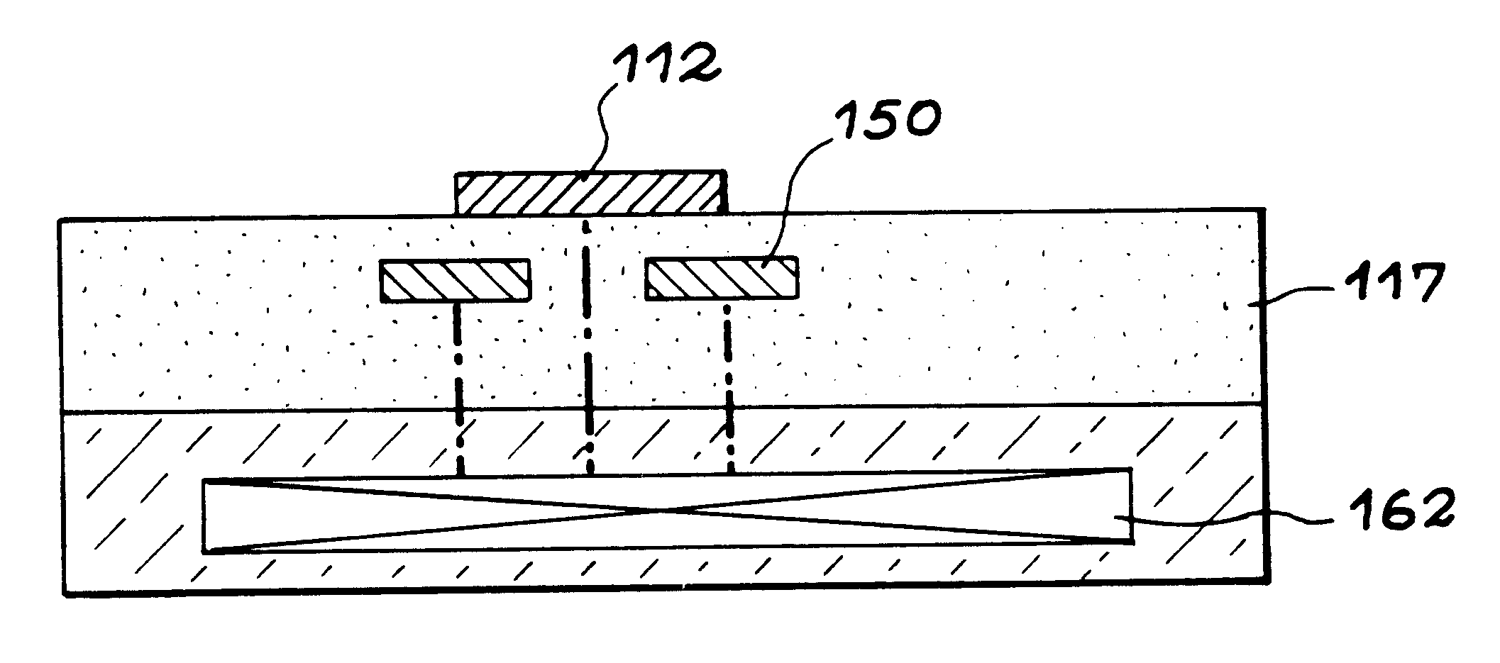
According to the device of the invention, the heating means may consist, for each electrode, of a conductive heating track disposed in the vicinity of the said electrode.
It is considered that the conductive heating track is disposed in the vicinity of an analysis electrode when the mean distance separating the conductive track from this electrode is less than the distance separating the conductive track from the other analysis electrodes of the chip.
In particular, each conductive heating track can be disposed so as to surround the electrode.
According to a variant, in which the electrodes are themselves configured in the form of conductive tracks, a conductive heating track can be respectively associated with at least one conductive track forming an electrode and then extending parallel to it.
The individual heating means may have electronic addressing circuits connected to addressing electrodes, and designed to selectively, in each conductive heating track, cause a current to flow co...
second embodiment
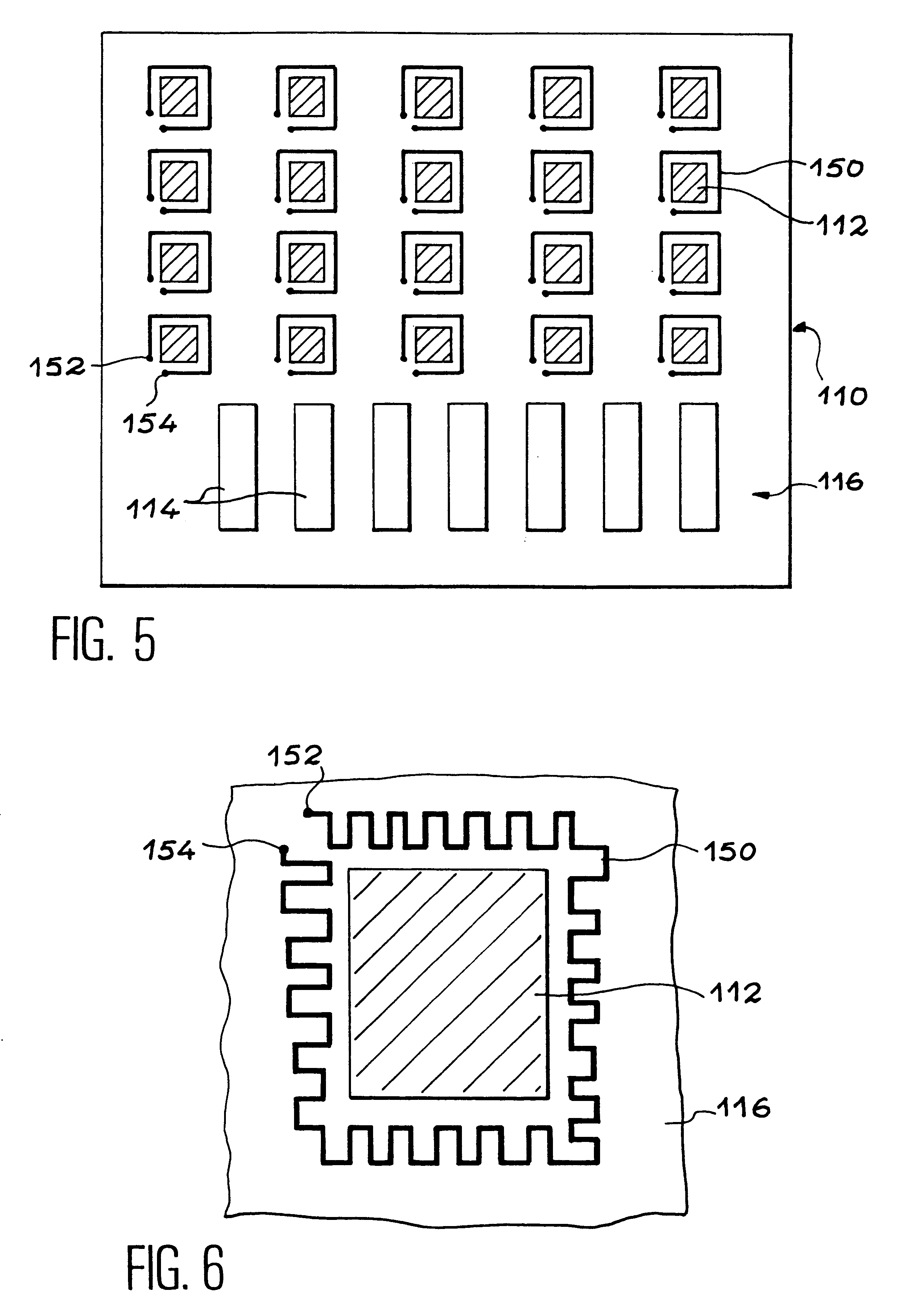
FIG. 12 shows the invention which does not require any conductive heating tracks or electrical addressing.
Chip 110 used for this embodiment of the invention consists simply of an isolating substrate 116 on which analysis electrodes 112 are formed. Incidentally, the substrate may also have counter electrodes, and addressing electrodes as described previously. It may also be coated with a thermal isolation layer making it possible to reduce the thermal exchanges between the electrodes.
The means of individual heating of analysis electrodes 112 consist of a laser source 170 and a network 172 of microlenses.
Network 172 of microlenses receives a light beam 174 from the laser. It is disposed opposite the analysis electrodes 112 of chip 110 so as to concentrate the light beam 174 selectively on electrodes 112, as indicated in FIG. 12.
The light beam concentrated on the electrodes makes it possible to heat them.
By way of example for a square analysis electrode of side 50 .mu.m, exposed to a l...
PUM
Property
Measurement
Unit
Density
aaaaa
aaaaa
Electrical conductor
aaaaa
aaaaa
Abstract
The invention concerns an analysis device including at least one chip (110) equipped with a plurality of analysis electrodes (112). In accordance with the invention, the device also includes means of individual heating (150) of the analysis electrodes.The invention can be used for the analysis of chemical or biological products, for example in an antigen / antibody recognition or DNA / DNA analysis.
Description
The present invention relates to an analysis device comprising an electronic chip equipped with a plurality of electrodes. Such a chip is used to constitute a miniaturized chemical or biological analysis cell. This is because each electrode of the chip can be coated individually with a compound or a material sensitive to a specific chemical or biological product.An analysis device in accordance with the invention can be used, for example, as a glucose measurer, or as a device for blood analysis or for analysis of various chemical or biological products.A particular application of the device of the invention in the field of molecular biology is that of antibody / antigen recognition. Similarly, the device can also be used in DNA chips.PRIOR ARTAn electronic chip for an analysis device as mentioned above may include several hundred electrodes each carrying a DNA probe. DNA probe means DNA molecules having a predetermined known sequence. The selective hybridization of DNA molecules in a ...
Claims
Application Information
Patent Timeline
Application Date:The date an application was filed.
Publication Date:The date a patent or application was officially published.
First Publication Date:The earliest publication date of a patent with the same application number.
Issue Date:Publication date of the patent grant document.
PCT Entry Date:The Entry date of PCT National Phase.
Estimated Expiry Date:The statutory expiry date of a patent right according to the Patent Law, and it is the longest term of protection that the patent right can achieve without the termination of the patent right due to other reasons(Term extension factor has been taken into account ).
Invalid Date:Actual expiry date is based on effective date or publication date of legal transaction data of invalid patent.

