Underfill preform interposer for joining chip to substrate

a preform interposer and chip technology, applied in the direction of printed circuit, sustainable manufacturing/processing, final product manufacturing, etc., can solve the problems of fatigue of solder joints, temperature excursions of the entire module, expansion and contraction of all of these components,

Inactive Publication Date: 2001-07-10
IBM CORP
View PDF20 Cites 70 Cited by
  • Summary
  • Abstract
  • Description
  • Claims
  • Application Information

AI Technical Summary

Benefits of technology

is to provide a method of assembling electron

Problems solved by technology

During normal operation, the entire module is subject to temperature excursions due to the functioning of the circuits on the chip, resistance heating of the solder joints, the wiring within the chip, and the wiring within the substrate.
This heating results in the expansion and contraction of all of these components as temperatures rise and fall.
ing. This mismatch places stresses on the solder joints, and over time results in the fatigue of the solder jo
ints. Eventually, continual stressing causes cracks to propagate completely across the solder joints leading to electrical failure of the electronic m
However, in many cases, this type of optimization is not sufficient to achieve a useful product life.
Although a proven means by which to enhance f

Method used


Image

  • Underfill preform interposer for joining chip to substrate
  • Underfill preform interposer for joining chip to substrate
  • Underfill preform interposer for joining chip to substrate

Examples


Embodiment Construction

)

In describing the preferred embodiment of the present invention, reference will be made herein to FIGS. 1-6 of the drawings in which like numerals refer to like features of the invention. Features of the invention are not necessarily shown to scale in the drawings.

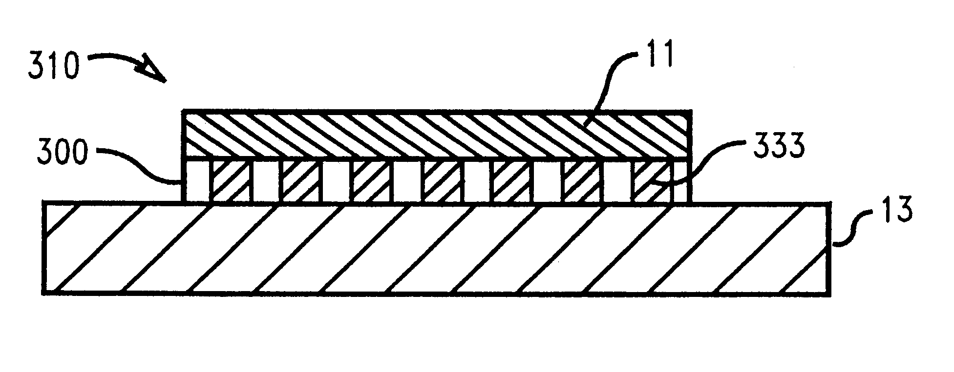
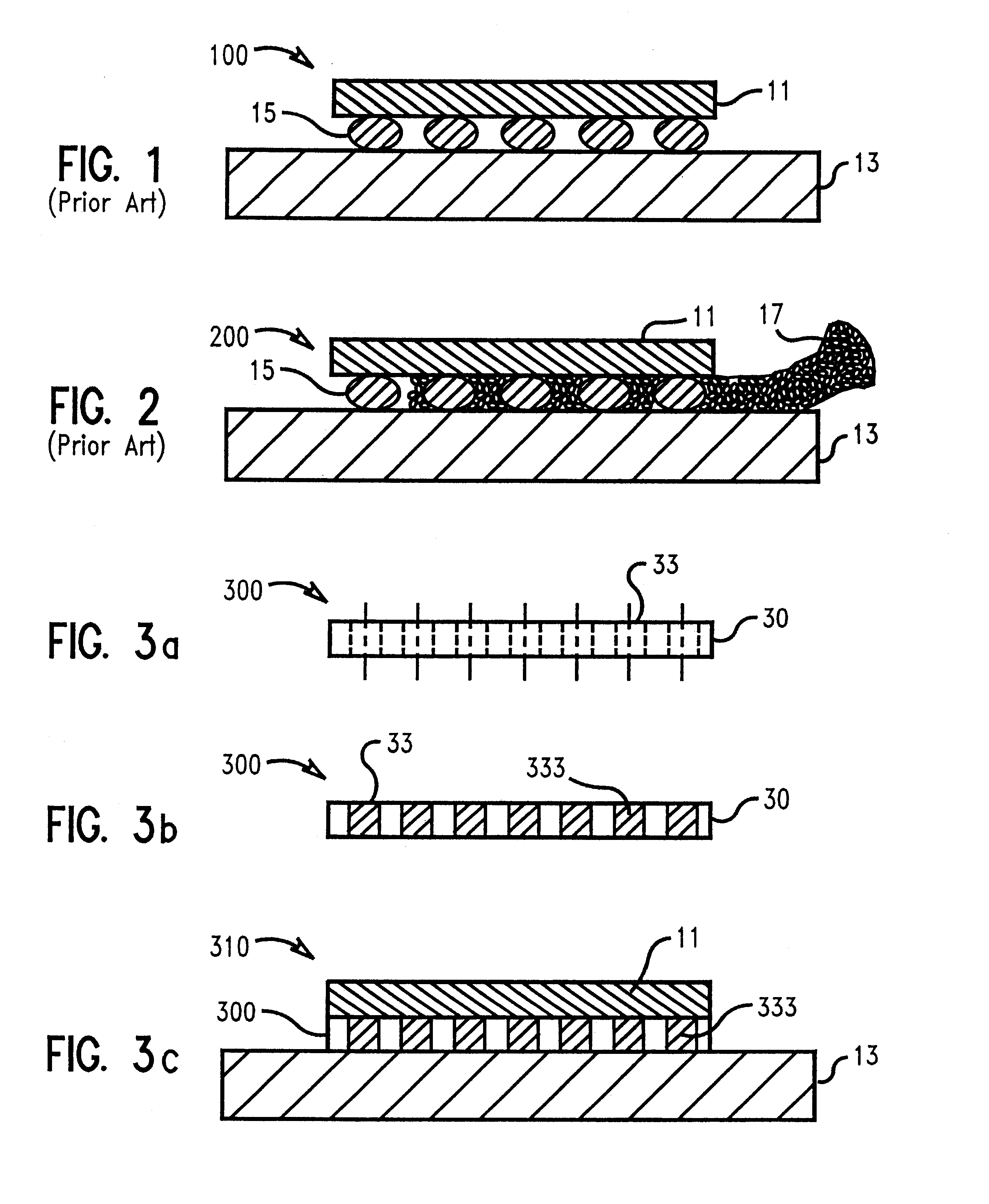
The present invention involves the use of a thin film interposer to make connections between a chip and a substrate for flip chip applications as depicted in FIGS. 3a-3c. The interposer 300 consists of a preformed laminate sheet 30, which is fabricated with multiple apertures or through-holes 33 as depicted in FIG. 3a. The laminate sheet 30 may comprise of an organic polymer such as polyimide, Kapton.RTM., Mylar.RTM., or any other material that will be stable at temperatures which are required to either join the interposer to the chip and the substrate, or to power the chip / substrate combination during normal operation.

The apertures 33 traverse the entire thickness of the laminate sheet 30. The apertures 33 may be formed ...


PUM


Abstract

An apparatus for and method of minimizing the thermo-mechanical fatigue of flip-chip packages. The interposer of the present invention, preferably comprising an organic polymer such as polyimide, contains apertures having conductive plugs inserted therein for joining a chip to a substrate in an electronic module utilizing flip-chip packaging. The interposer is selected to provide optimum spacing between the chip and substrate having a coefficient of thermal expansion adapted to the thermal cycling temperature extremes of the module components. The interposer may comprise an inner core with two adhesive outer layers which may comprise different materials to promote adhesion at their respective interfaces within a module. Conductive plugs are disposed within the apertures of the interposer comprising of a first and second solder or comprising a conductive plug having top and bottom surfaces coated with a conductive adhesive. Preferably, the first solder is disposed within an interior of the apertures and the second solder is disposed within an exterior of the apertures such that the first solder is between a first portion and a second portion of the second solder. Upon reflow, the second solder is reflowed while the first solder remains solid.

Description

Aspects of the present invention are related to subject matter disclosed in co-pending applications entitled "Process for Forming Cone Shaped Solder for Chip Interconnection," Attorney Docket No. FI9-97-060, and "Dielectric Interposer for Chip to Substrate Soldering," Attorney Docket No. FI9-98-129 filed on even date herewith and assigned to the assignee of the present invention.1. Field of the InventionThis invention relates to the assembly of electronic modules, and in particular, to a structure and method of minimizing the thermo-mechanical fatigue that typically occurs as a result of the mismatch in the coefficients of thermal expansion of a chip and a substrate when they are joined in a flip-chip arrangement. It has wide applicability, including extension to very small joints and very densely populated arrays.2. Description of Related ArtMulti-layer ceramic electronic components are typically joined together by soldering pads on a surface of one of the electronic components to ...

Claims


Application Information

Patent Timeline
IPC IPC(8): H01L21/60H01L21/02H01L21/56H05K3/34
CPCH01L21/563H01L24/11H05K3/3436H01L24/28H01L2224/32225H01L2224/16225H01L2924/014H01L2924/01033H01L2924/01006H05K2201/10977H05K2201/10674H05K2201/10378H01L2924/14H01L2224/13099H01L2224/73203H01L2224/73204H01L2224/83102H01L2224/92125H01L2924/01004H01L2924/01005H01L2924/01027H01L2924/01029H01L2924/0105H01L2924/01075H01L2924/01078H01L2924/01082H01L2924/01322H01L2924/3512H01L2924/00H01L2924/15787Y02P70/50
Inventor BENENATI, JOSEPH A.CHEN, WILLIAM T.FANTI, LISA A.HOWELL, WAYNE J.KNICKERBOCKER, JOHN U.
Owner IBM CORP
Why Eureka
Try Eureka