Method of making air gap isolation by making a lateral EPI bridge for low K isolation advanced CMOS fabrication

a technology of lateral epi bridge and low k isolation, applied in the field of isolation structure, can solve the problems of bird's beak structure formation, substrate surface exposure, and difficult to achieve the effect of reducing the thickness of the device, and reducing the packing density of the device in the integrated circui

Inactive Publication Date: 2001-07-31
GLOBALFOUNDRIES INC
View PDF4 Cites 72 Cited by
  • Summary
  • Abstract
  • Description
  • Claims
  • Application Information

AI Technical Summary

Problems solved by technology

The formation of bird's beak structures is problematic in a number of ways.
To begin with, bird's beak formation can create significant limitations on the packing density of devices in an integrated circuit.
In addition, the very shape of a bird's beak can result in the exposure of the substrate surface during subsequent overetching to open contacts for metallization.
This can result in the source of the transistor becoming shorted to the well region when the metal interconnect film is deposited.
This problem may be particularly acute in CMOS circuits where shallower junctions are used, due to the higher propensity for the exposure of the well regions.
While some improvement in the formation of bird's beak structures has occurred as a result of the introduction of techniques such as the etchback of portions of the field oxide structures, deposition of a silicon nitride layer without a pad oxide layer, and use of a thin pad oxide covered with polysilicon, the difficulties associated with bird's beak formation have not been completely eliminated.
Although conventional trench and refill isolation techniques eliminate the difficulties associated with bird's beak formation in LOCOS processes, there are nevertheless difficulties associated with...

Method used


Image

  • Method of making air gap isolation by making a lateral EPI bridge for low K isolation advanced CMOS fabrication
  • Method of making air gap isolation by making a lateral EPI bridge for low K isolation advanced CMOS fabrication
  • Method of making air gap isolation by making a lateral EPI bridge for low K isolation advanced CMOS fabrication

Examples


Embodiment Construction

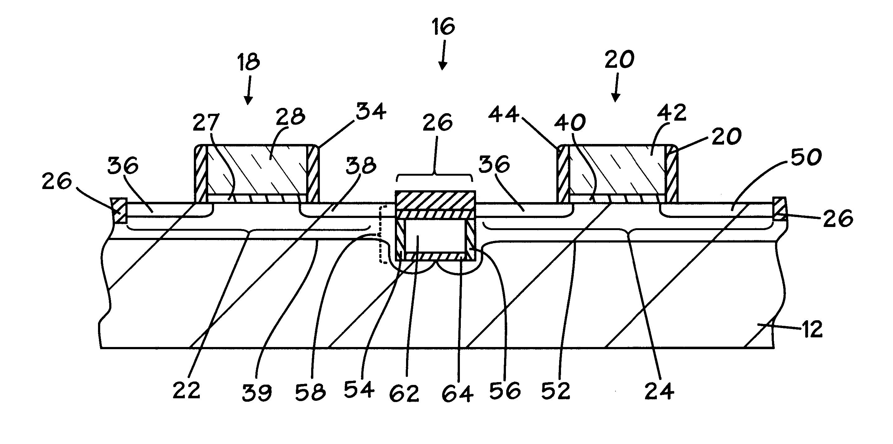
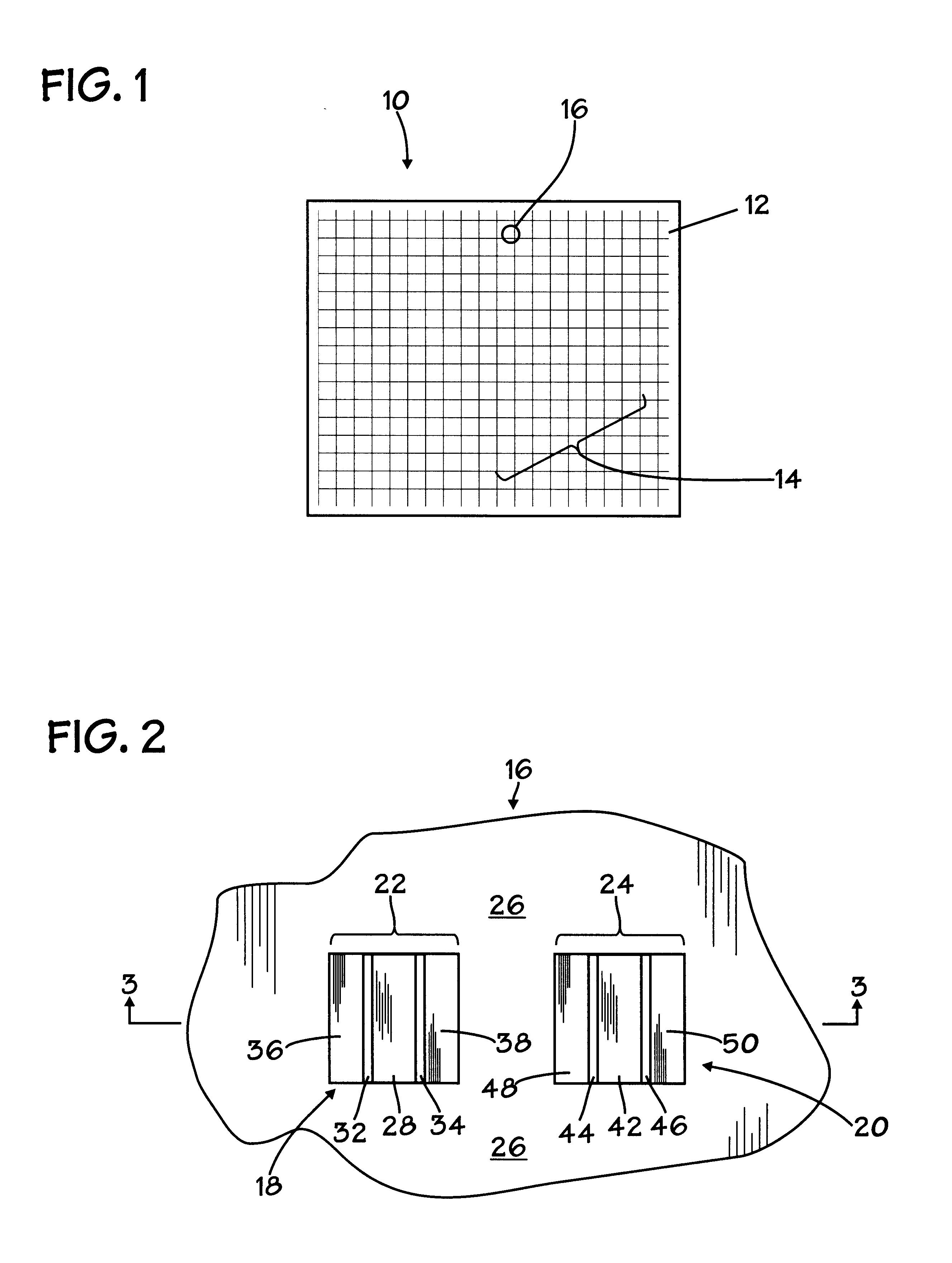
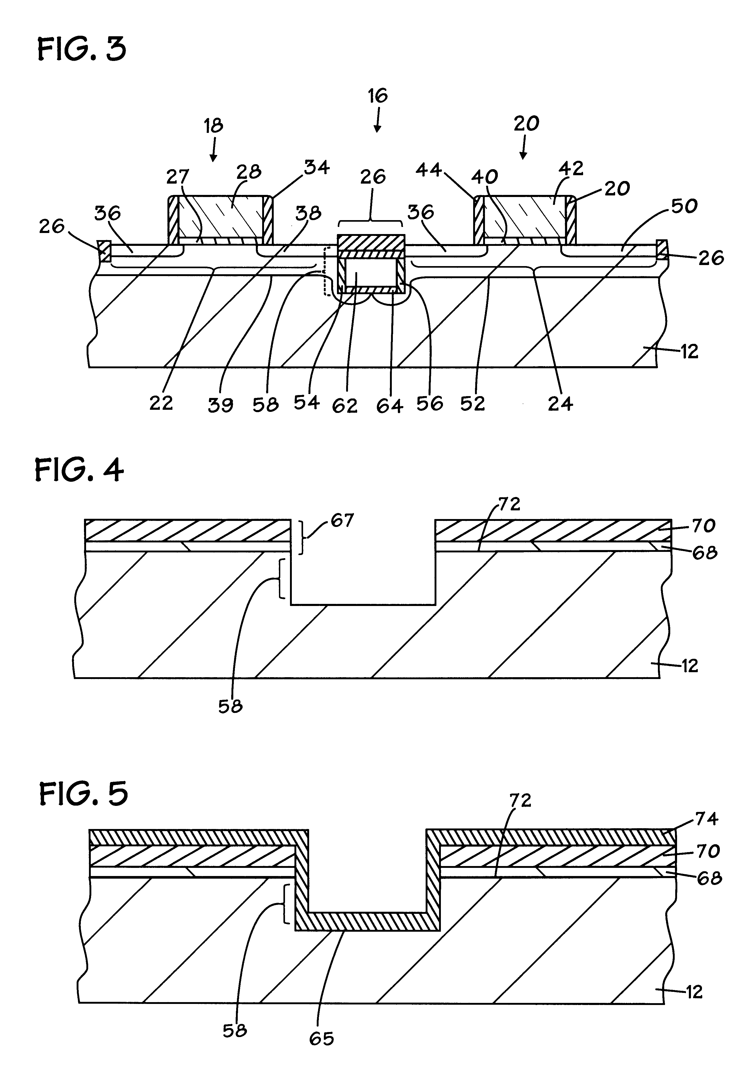
In the drawings described below, reference numerals are generally repeated where identical elements appear in more than one figure. Turning now to the drawings, and in particular to FIG. 1, there is shown a plan view of an exemplary embodiment of an integrated circuit 10 implemented on a semiconductor substrate 12. The substrate 12 may be n-doped silicon, p-doped silicon, silicon-on-insulator or other suitable substrate material. The integrated circuit 10 includes a plurality of circuit devices 14 that can include transistors, capacitors, resistors or the like. A very small portion of the integrated circuit 10 is designated 16 and is shown in a highly magnified plan view in FIG. 2. Various metallization and interlevel dielectric layers have been peeled away in FIG. 2 to reveal two exemplary circuit devices 18 and 20 that are formed on respective active areas 22 and 24 of the substrate 12. As used herein, the terms "formed on" or "disposed on" should be construed to include the possi...


PUM


Abstract

An isolation structure and a method of making the same are provided. In one aspect, the method includes the steps of forming a trench in a substrate and forming a first insulating sidewall in the trench and a second insulating in the trench in spaced-apart relation to the first insulating sidewall. A bridge layer is formed between the first and the second sidewalls. The bridge layer, the first and second sidewalls, and the substrate define an air gap in the trench. The isolation structure exhibits a low capacitance in a narrow structure. Scaling is enhanced and the potential for parasitic leakage current due to non-planarity is reduced.

Description

1. Field of the InventionThis invention relates generally to semiconductor processing, and more particularly to an isolation structure and to a method of making the same incorporating an air gap.2. Description of the Related ArtThe implementation of integrated circuits involves connecting isolated circuit devices through specific electrical pathways. Where integrated circuits are implemented in silicon, it is necessary, therefore, to initially isolate the various circuit devices built into the silicon substrate from one another. The circuit devices are thereafter interconnected to create specific circuit configurations through the use of global interconnect or metallization layers and local interconnect layers.Local oxidation of silicon ("LOCOS") and trench and refill isolation represent two heavily used isolation techniques for both bipolar and metal oxide semiconductor ("MOS") circuits. In a conventional semi-recessed LOCOS process, a thin pad oxide layer is thermally grown on a s...

Claims


Application Information

Patent Timeline
IPC IPC(8): H01L21/70H01L21/764H01L21/8238
CPCH01L21/823878H01L21/764
Inventor GARDNER, MARK I.HAUSE, FREDERICK N.MAY, CHARLES E.
Owner GLOBALFOUNDRIES INC
Why Eureka
Try Eureka