Method for wavelength compensation in semiconductor photonic IC

Inactive Publication Date: 2001-08-14
NORTHLIGHT OPTRONICS AB
View PDF3 Cites 7 Cited by
  • Summary
  • Abstract
  • Description
  • Claims
  • Application Information

AI Technical Summary

Benefits of technology

An advantage with the present invention is that an apparatus used for selective area growth processes resulting in a varied growth across the substrates still may be used with an increased yield.

Problems solved by technology

This results in a low yield of functioning devices on the substrate, since the wavelength difference, so called detuning, between the laser and the modulator is important.

Method used


Image

  • Method for wavelength compensation in semiconductor photonic IC
  • Method for wavelength compensation in semiconductor photonic IC
  • Method for wavelength compensation in semiconductor photonic IC

Examples


Embodiment Construction

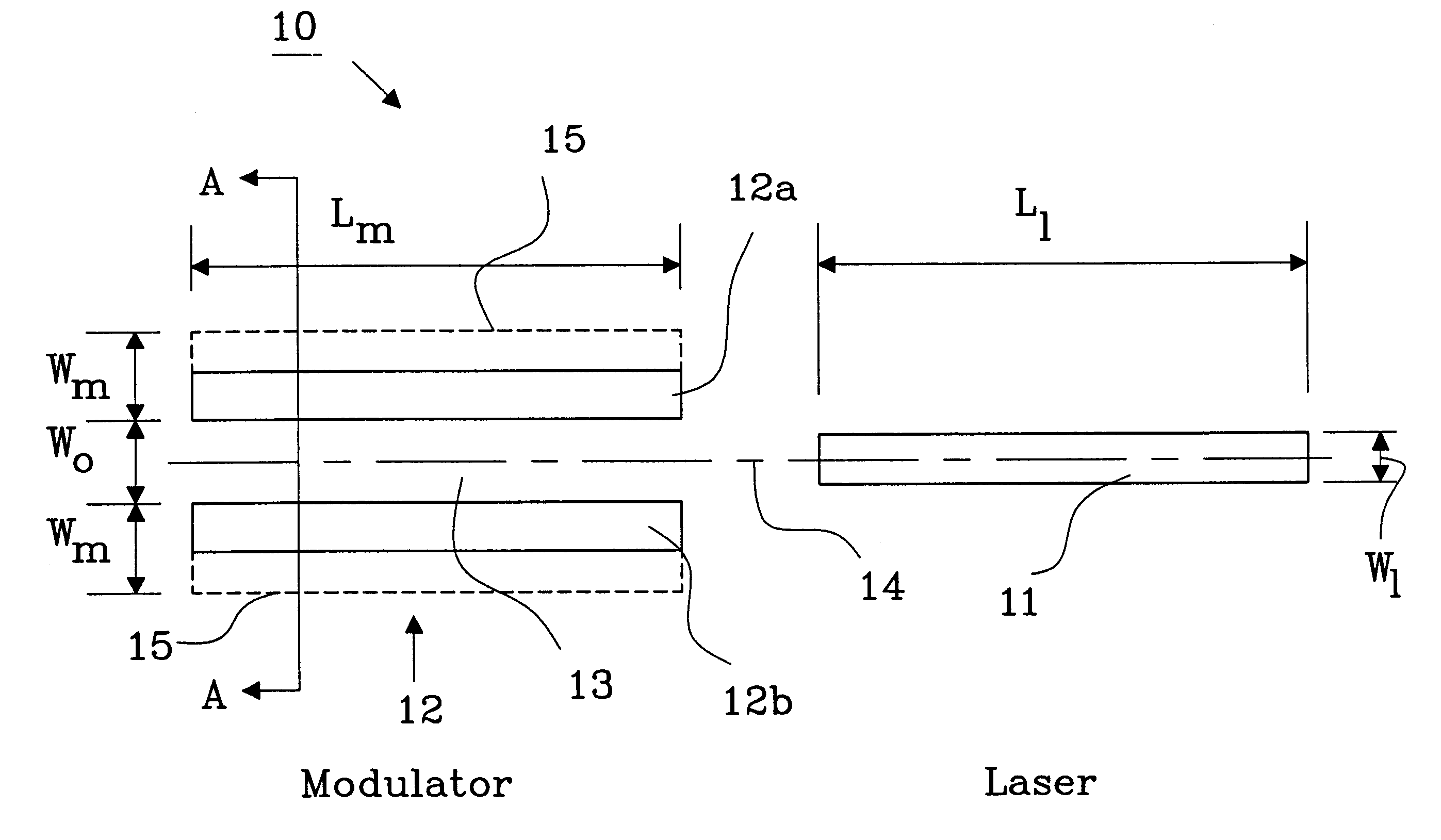
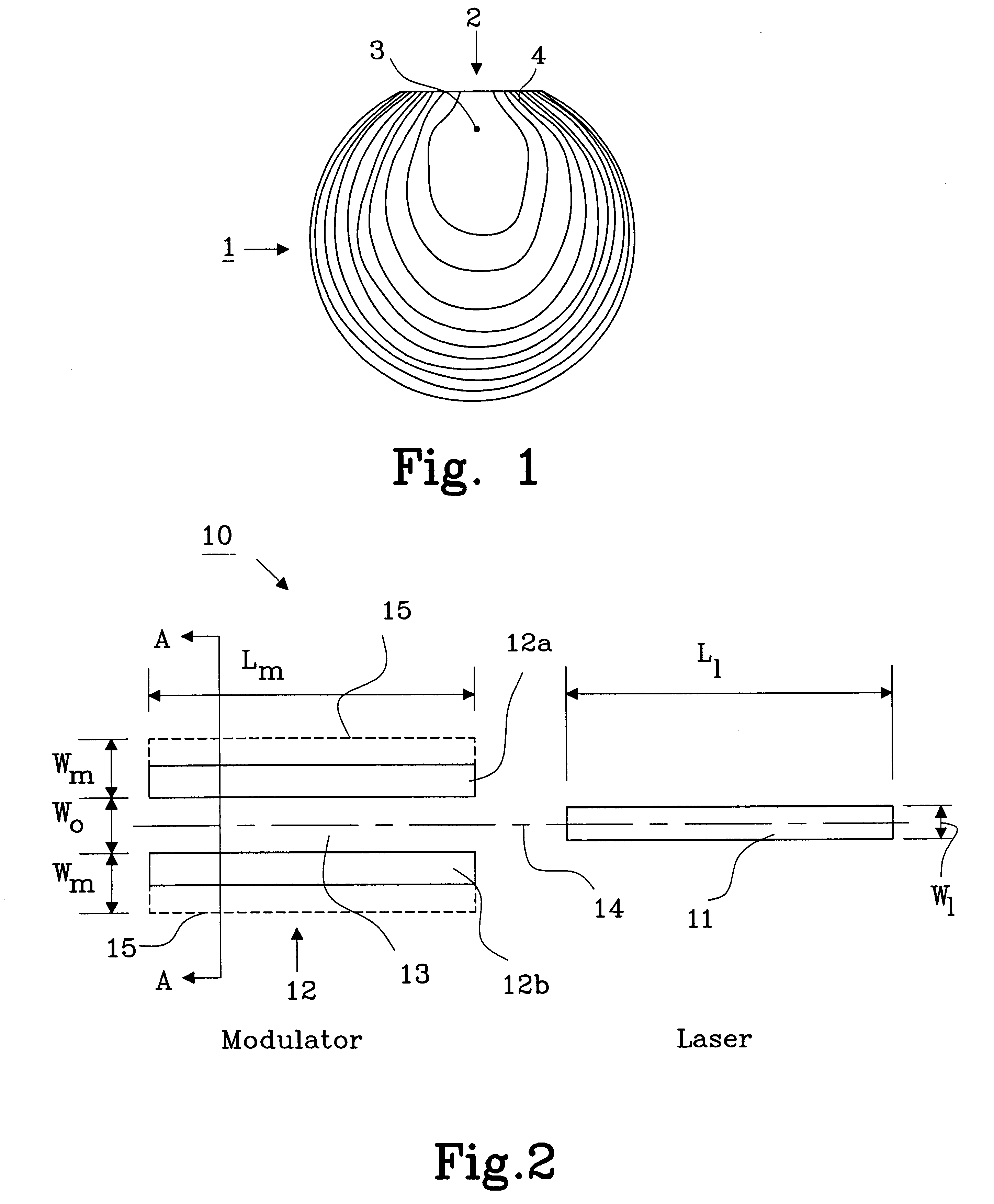
FIG. 1 shows a top view of a wafer 1 illustrating an optical waveguide layer in a modulator having variations in band-gap energy across the wafer. This variation is due to the type of reactor used in manufacturing the layer. As described before this occurs in a reactor where the wafer is fixedly mounted during the epitaxial growth process and the used gases are introduced from one direction 2. The variations are measured with a photo luminescence measuring apparatus and the result is presented in decreasing wavelength compared to a highest wavelength, which is obtained at a reference point 3, near the top middle of the wafer. The increasing wavelength difference is divided into intervals of 5 nm, where each line 4 indicates a 5 nm drop from the previous line counting from the reference point 3. The variations across the wafer 1 is in this example more than 45 nm, which is unacceptable when manufacturing a modulator that is working with a semiconductor laser, having a fixed emitting ...


PUM


Abstract

The present invention relates to a method for manufacturing a plurality of semiconductor photonic integrated circuit comprising at least a laser and a modulator connected optically to one another. Each laser and modulator has a waveguide layer being implemented on a single substrate, where said modulator is formed by use of a selective area growth technique. By providing modulator masking parts with selectable width to compensate a difference in band-gap energy in the waveguide layer between the laser and the modulator a approximate uniform difference in band-gap energy between the optically connected laser and modulator may be obtained.

Description

The present invention relates to a method for wavelength compensation in a photonic device manufactured on a semiconductor substrate using selective area growth. The invention further relates to an integrated circuit comprising a photonic device manufactured by this method.BACKGROUND TO THE INVENTIONThere exists what is known as selective area growth (SAG) technique that utilises insulating film patterning masks in integrally fabricating, on the same semiconductor substrate, such semiconductor photonic devices as semiconductor laser, optical modulator, optical switch, photo detector and optical amplifier of different functions. The selective area growth technique involves primarily forming insulating film patterning masks over the semiconductor substrate so as to permit vapour phase growth of semiconductor crystals in unmasked areas, i.e. exposed areas of the substrate. During manufacture of target semiconductor photonic devices, the width of the insulating film mask and that of the...

Claims


Application Information

Patent Timeline
IPC IPC(8): H01L33/00H01S5/00H01S5/026H01S5/20
CPCH01L33/0062H01S5/0265H01S5/2077H01L27/15
Inventor BENDZ, ESKILLUNDQVIST, LENNART
Owner NORTHLIGHT OPTRONICS AB
Why Eureka
Try Eureka