Line path determining method and delay estimating method

a delay estimation and path determining technology, applied in the direction of cad circuit design, program control, instruments, etc., can solve the problem that the proportion of delay dependent on the line capacitance is relatively increased in the delay of the entire integrated circuit, and cannot be always decreased in output load capacitance of a cell, so as to achieve the effect of removing timing errors by modifying routing

Inactive Publication Date: 2001-09-18
PANASONIC CORP
View PDF12 Cites 15 Cited by
  • Summary
  • Abstract
  • Description
  • Claims
  • Application Information

AI Technical Summary

Benefits of technology

The object of the invention is providing a line path determining method in which line paths can be determined in rough routing with a timing error eliminated through estimation of a line capacitance in consideration of the influence of adjacent lines.

Problems solved by technology

However, since the capacitance between adjacent lines is increased due to the refinement of the lines, the output load capacitance of a cell cannot be always decreased, and hence, the proportion of delay depending upon the line capacitance is relatively increased in the delay of the entire integrated circuit.
However, the conventional methods of determining a line path have the following problems:
In the first conventional method, since a line capacitance is calculated in consideration of the influence of an adjacent line after completely generating the routing pattern in detail on the basis of the detailed routing, when there is a timing error, it is very difficult to remove the timing error by modifying the routing.
Specifically, the amount of data to be dealt with for modifying the routing is so large that the process takes a long period of time, and in some cases, the calculating process cannot be converged and the routing cannot be modified.
Alternatively, in the second conventional method, since a line is assumed to be allocated to an interconnect layer with the maximum unit capacitance in the net against the timing constraint, the line capacitance is likely to be excessively estimated.
Also, since an adjacent line is not considered in the estimation of the line capacitance, even when no timing error is caused in the rough routing process, a timing error can be occasionally caused due to an adjacent line after detailed routing.

Method used


Image

  • Line path determining method and delay estimating method
  • Line path determining method and delay estimating method
  • Line path determining method and delay estimating method

Examples


Embodiment Construction

An embodiment of the invention will now be described with reference to the accompanying drawings.

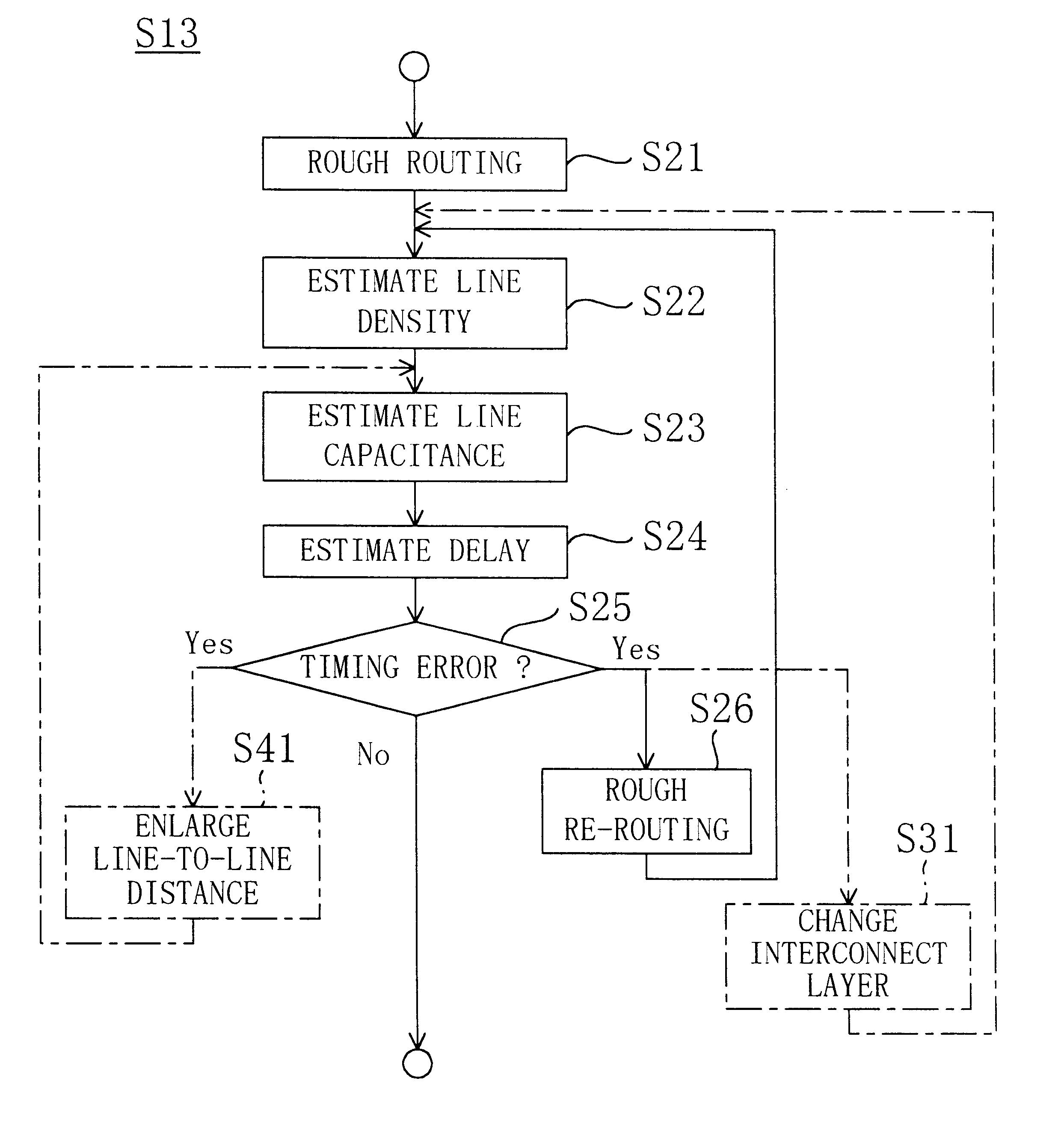
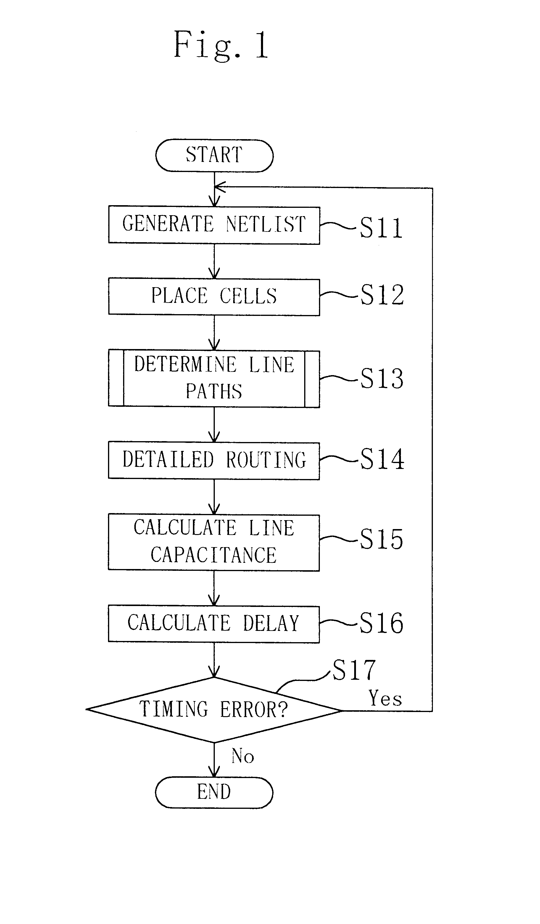
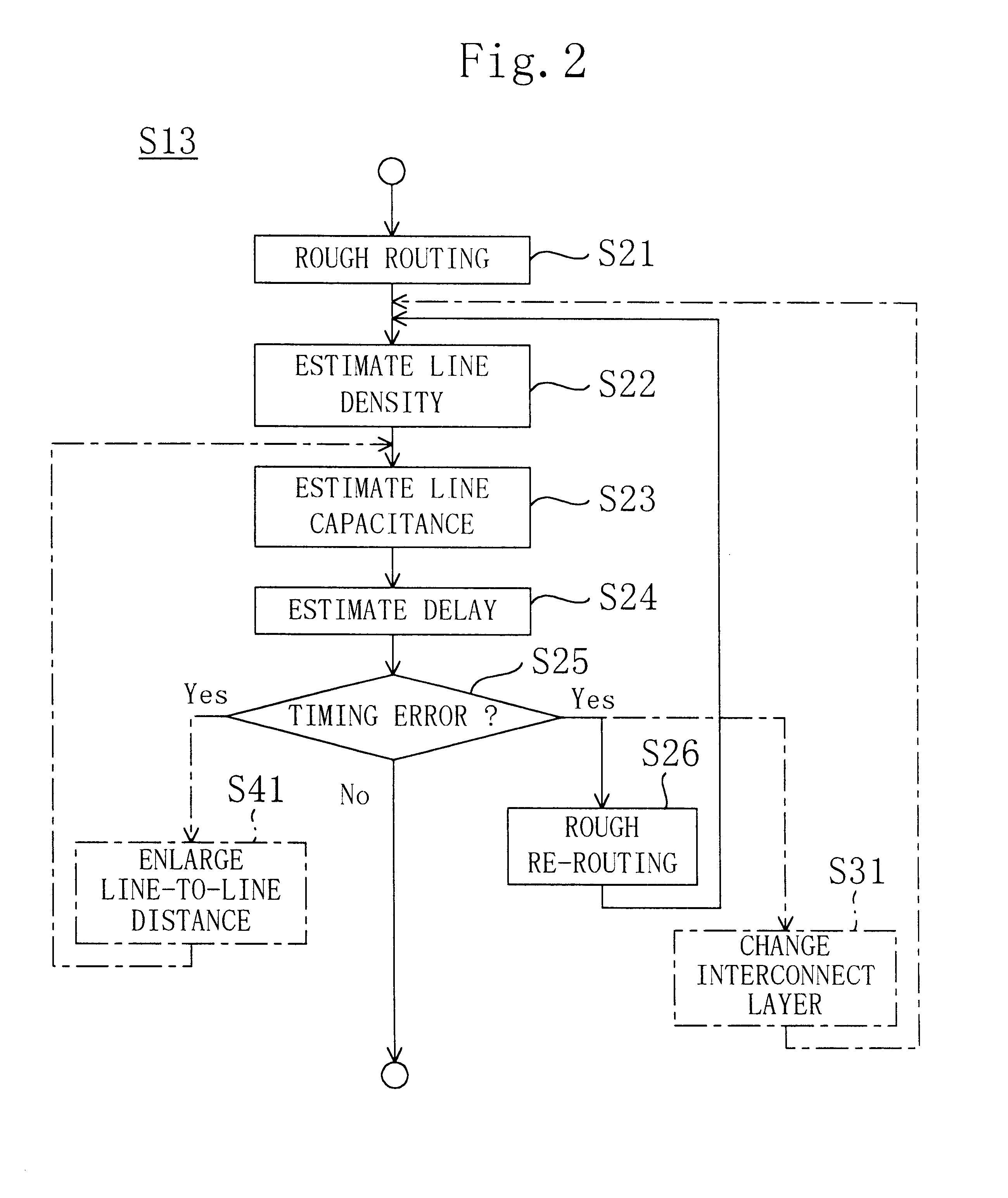
FIG. 1 is a flowchart for showing procedures in layout design for an integrated circuit. In FIG. 1, S11 indicates a netlist making step of making a netlist describing connection between respective cells in a target integrated circuit; S12 indicates a cell placing step of placing each cell described in the netlist made in the netlist making step S11; S13 indicates a line path determining step of determining line paths between the cells placed in the cell placing step S12; S14 indicates a detailed routing step of generating a routing pattern through detailed routing; S15 indicates a line capacitance calculating step of calculating a capacitance between lines on the basis of the routing pattern generated in the detailed routing step S14; and S16 indicates a delay time calculating step of calculating a delay time of the integrated circuit. Also, S17 indicates a step of verifying whether or n...


PUM


Abstract

A line capacitance is estimated in consideration of an influence of an adjacent line in rough routing, so that line paths can be determined so as to be free from a timing error. A routing graph is generated from a target integrated circuit, and line paths of cell-to-cell lines are initially determined on the basis of a passage cost set with regard to each of edges of the routing graph. With regard to each edge of the routing graph, the number of cell-to-cell lines passing through the edge is obtained as a line density, and a line capacitance of each line path in view of the influence of an adjacent line is estimated on the basis of the line density. It is verified whether or not there is a timing error with a delay time estimated, and when the integrated circuit does not satisfy a predetermined timing constraint, the line paths are re-determined with the passage cost of each edge allowed to be affected by the line capacitance. Alternatively, allocation to an interconnect layer is changed or a line-to-line distance is increased, so that the integrated circuit can satisfy the timing constraint.

Description

BACKGROUND OF THE INVENTIONThe present invention relates to a layout design technique for integrated circuits, and more particularly, it relates to methods of determining a line path and estimating delay in rough routing of semi-custom LSIs such as an ASIC.In the recent manufacturing technique for semiconductor integrated circuits, transistors and lines have been more and more refined. In accordance with the refinement, the delay time of a transistor itself tends to be decreased. However, since the capacitance between adjacent lines is increased due to the refinement of the lines, the output load capacitance of a cell cannot be always decreased, and hence, the proportion of delay depending upon the line capacitance is relatively increased in the delay of the entire integrated circuit.Accordingly, in order to guarantee an operation timing, the recent layout design for an integrated circuit requires a method of precisely estimating a line capacitance in consideration of an adjacent li...

Claims


Application Information

Patent Timeline
Patent Type & Authority Patents(United States)
IPC IPC(8): G06F17/50H01L21/82
CPCG06F17/5077G06F17/5022G06F30/33G06F30/394G06F30/3308
Inventor YAMAGUCHI, RYUICHIKUROKAWA, KEIICHI
Owner PANASONIC CORP
Why Eureka
Try Eureka