Nonvolatile semiconductor memory device

a nonvolatile, memory device technology, applied in the direction of instruments, coding, code conversion, etc., can solve the problems of low voltage value of power supply voltage, limited processing time of electronic devices, and high integration of nonvolatile memory such as flash memory, so as to shorten processing time

Inactive Publication Date: 2012-11-22
SHARP KK
View PDF6 Cites 13 Cited by
  • Summary
  • Abstract
  • Description
  • Claims
  • Application Information

AI Technical Summary

Benefits of technology

[0016]The present invention has been made in the light of the above problems, and an object of thereof is to provide a nonvolatile semiconductor memory device t...

Problems solved by technology

Because a volatile memory such as a DRAM requires a refresh operation, reduction of power consumption is difficult, and a using time of electronics devices is limited.
Further, a nonvolatile memory such as a flash memory has a problem in its high integration because of a limit to miniaturization.
However, along with miniaturization and integration in a semiconductor process, a voltage value of a power supply voltage tends to become small.
Further, to realize a high-speed read process, it is difficult to reduce a read current that is used for the read process.
Therefore, it becomes difficult to secure a sufficient difference between the write voltage and the read voltage.
That is, along with miniaturization and integration of elements, when it is not possible to secure a sufficient difference between the write voltage and the read voltage, there is a problem in that a risk of occurrence of an erroneous w...

Method used


Image

  • Nonvolatile semiconductor memory device
  • Nonvolatile semiconductor memory device
  • Nonvolatile semiconductor memory device

Examples


first embodiment

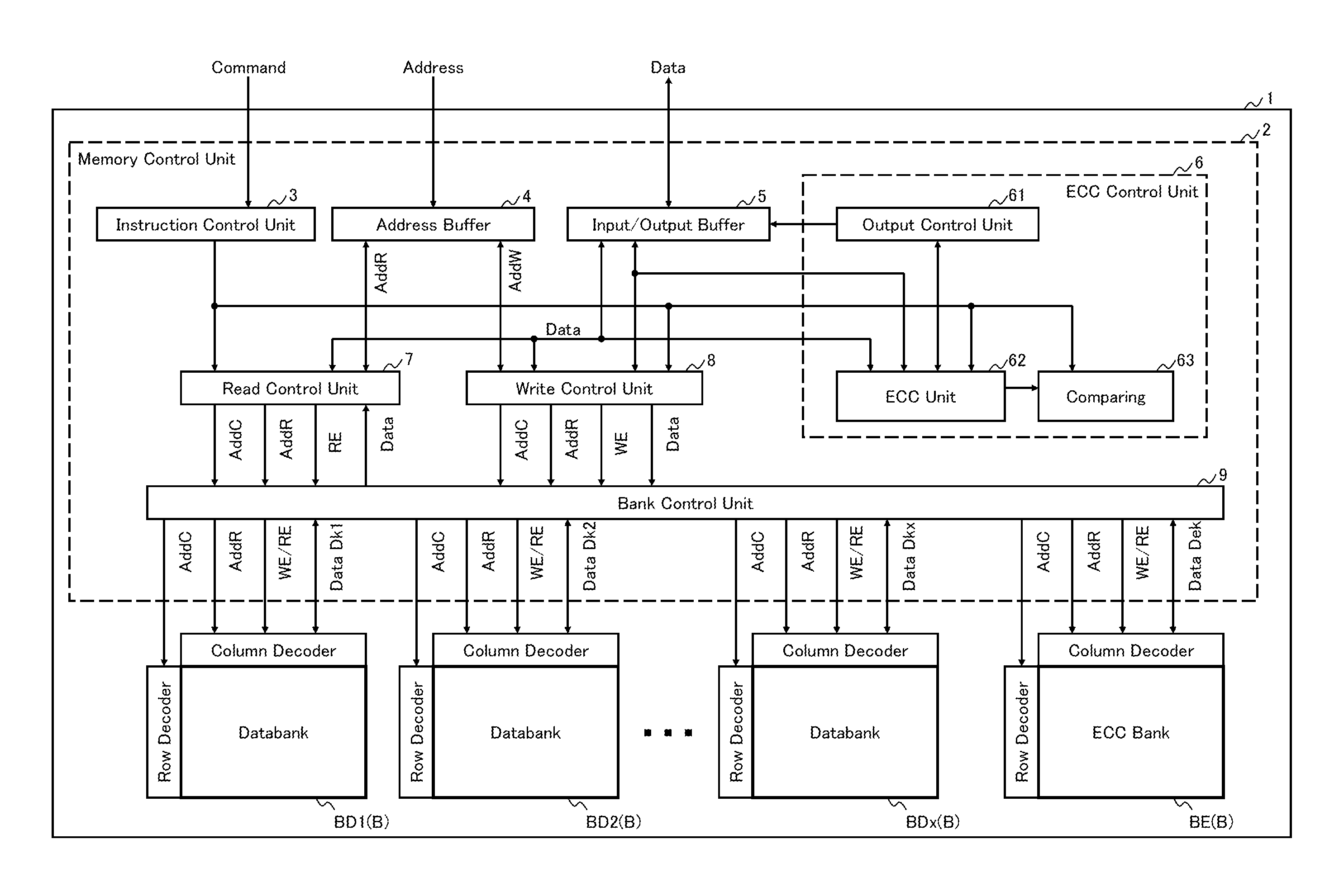
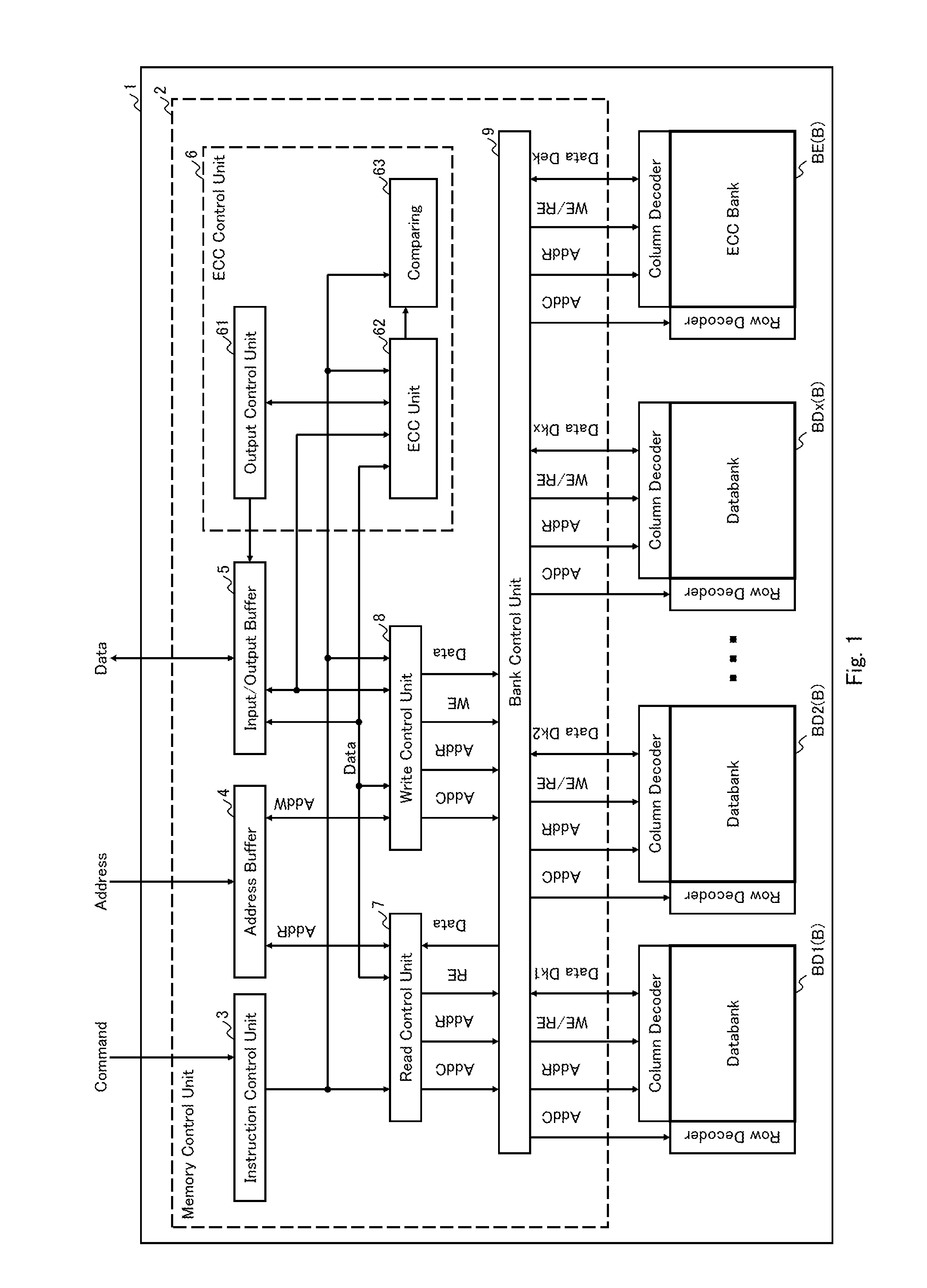
[0032]A device according to a first embodiment of the present invention is described with reference to FIGS. 1 to 4.

[0033]First, a configuration of a device 1 of the present invention is described with reference to FIGS. 1 and 2. In the present embodiment, the device 1 of the present invention is configured to perform a write process SW by receiving a write request from a CPU (not shown) and perform a read process SR by receiving a read request, and further includes a burst function that continuously performs a plurality of write requests or read requests.

[0034]As shown in FIG. 1, the device 1 of the present invention is configured to include a memory cell array that includes databanks BD1 to BDx (x is an integer equal to or larger than two) for storing data and an ECC bank BE for storing an error correction code, and a memory control unit 2 that performs various controls to the memory cell array.

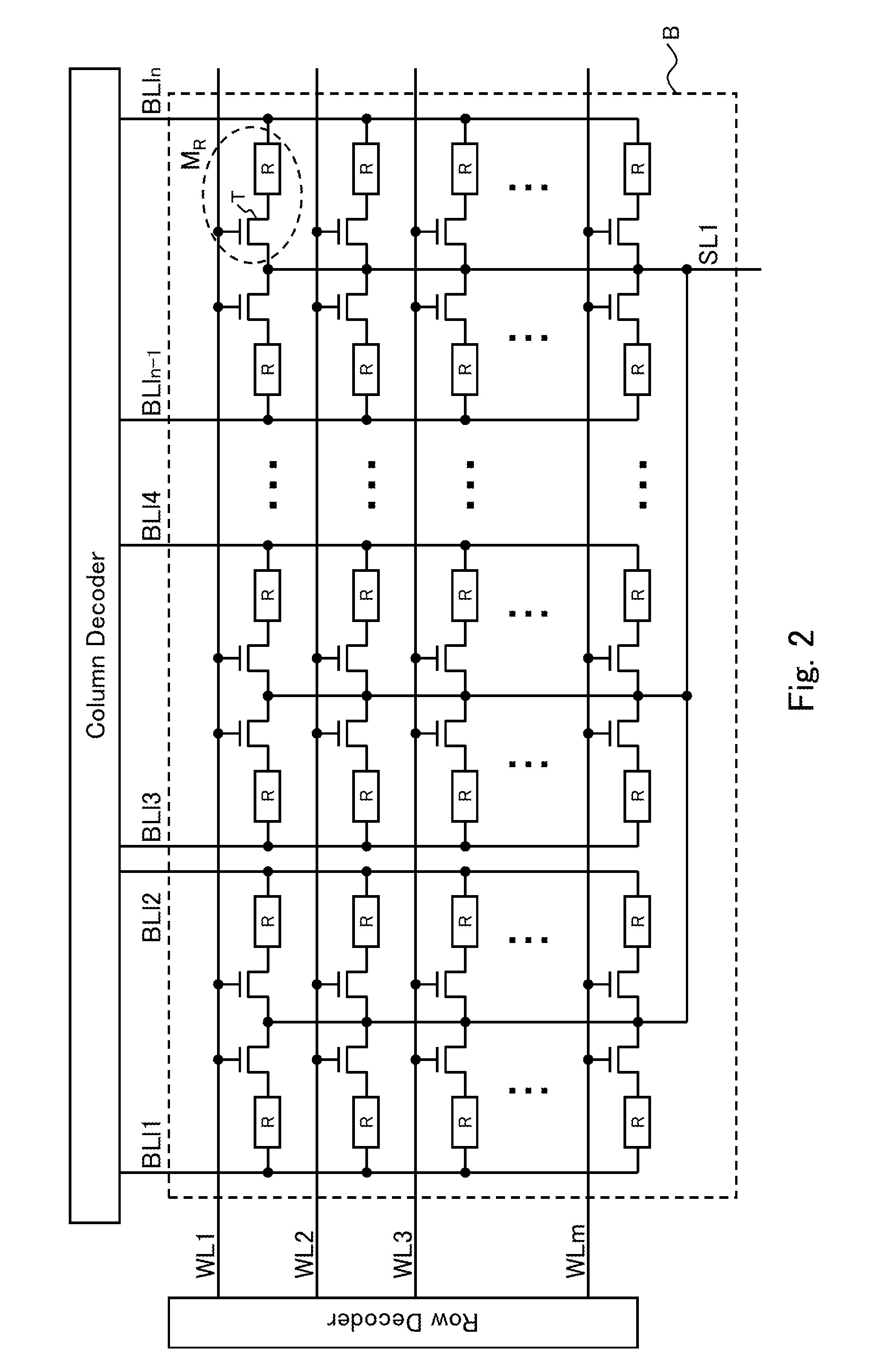
[0035]As shown in FIG. 2, the memory cell array is configured to include a plurality of...

second embodiment

[0057]The device 1 according to a second embodiment of the present invention is described with reference to FIGS. 1 to 4. While a case where the encode process SW is performed to the write data DW is described in the first embodiment, a case where the encode process SW is performed to divided data Dk1 to Dkx (k=1 to h) is described in the present embodiment.

[0058]The write process SW in the present embodiment is described with reference to FIG. 3. In the present embodiment, a case where a plurality of write requests CW1 to CWh are continuously performed by the burst function is described, in a similar manner to that of the first embodiment.

[0059]Upon receiving the write requests CW1 to CWh to the memory cell array issued from the CPU, the instruction control unit 3 first starts execution of the write process SW1 by controlling the write control unit 8 and the ECC control unit 6, based on the write request CW1, in a similar manner to that of the first embodiment.

[0060]When the write ...


PUM


Abstract

The present invention provides a nonvolatile semiconductor memory device that can optimize a timing of performing an error detection and correction process to shorten a processing time. Upon receiving a write request to a memory cell array including a variable resistive element where information is stored based on a resistance state of a variable resistor, an input/output buffer outputs write data to a write control unit and an ECC control unit. The write control unit performs a data write process of writing divided data, obtained by dividing the write data into a predetermined number of data, to the databanks. The ECC control unit generates a first error correction code by performing an error correction code generation process to the write data or the divided data, in parallel with the data write process. The write control unit performs a code write process of writing first test data into an ECC bank.

Description

CROSS REFERENCE TO RELATED APPLICATION[0001]This Nonprovisional application claims priority under 35 U.S.C. §119(a) on Patent Application No. 2011-110611 filed in Japan on May 17, 2011 the entire contents of which are hereby incorporated by reference.BACKGROUND OF THE INVENTION[0002]1. Field of the Invention[0003]The present invention relates to a nonvolatile semiconductor memory device that includes a memory cell array including a plurality of memory cells each including a variable resistive element which stores information by shifting between a plurality of states an electric resistance of a variable resistor sandwiched between a first electrode and a second electrode, by applying a voltage pulse between the first electrode and the second electrode.[0004]2. Description of the Related Art[0005]In portable electronics devices or mobile devices, a volatile memory such as a low-cost DRAM having a small number of parts and a nonvolatile memory such as a large-capacity and low-cost flas...

Claims


Application Information

Patent Timeline
IPC IPC(8): G11C29/04G06F11/16
CPCG06F11/1048G11C13/0002G11C13/004G11C2029/0411G11C13/0069G11C29/52G11C13/0061
Inventor ISHIHARA, KAZUYATABUCHI, YOSHIAKI
Owner SHARP KK
Why Eureka
Try Eureka