Design system of integrated circuit and its design method and program

Inactive Publication Date: 2005-03-22
FUJITSU LTD
View PDF6 Cites 13 Cited by
  • Summary
  • Abstract
  • Description
  • Claims
  • Application Information

AI Technical Summary

Benefits of technology

[0027]According to thus-structured present invention, the delay information is immediately presumed from the modified circuit information to recover the timing error. This allows carr

Problems solved by technology

In recent years, the layout design, which organizes the arrangement of respective circuit elements (e.g. logic gates) composing the integrated circuit on a chip and wiring between these circuit elements, has been complicated as the integrated circuit becomes large in scale and high-speed and the process becomes refined.
The timing adjustment to recover the set-up erro

Method used


Image

  • Design system of integrated circuit and its design method and program
  • Design system of integrated circuit and its design method and program
  • Design system of integrated circuit and its design method and program

Examples


Embodiment Construction

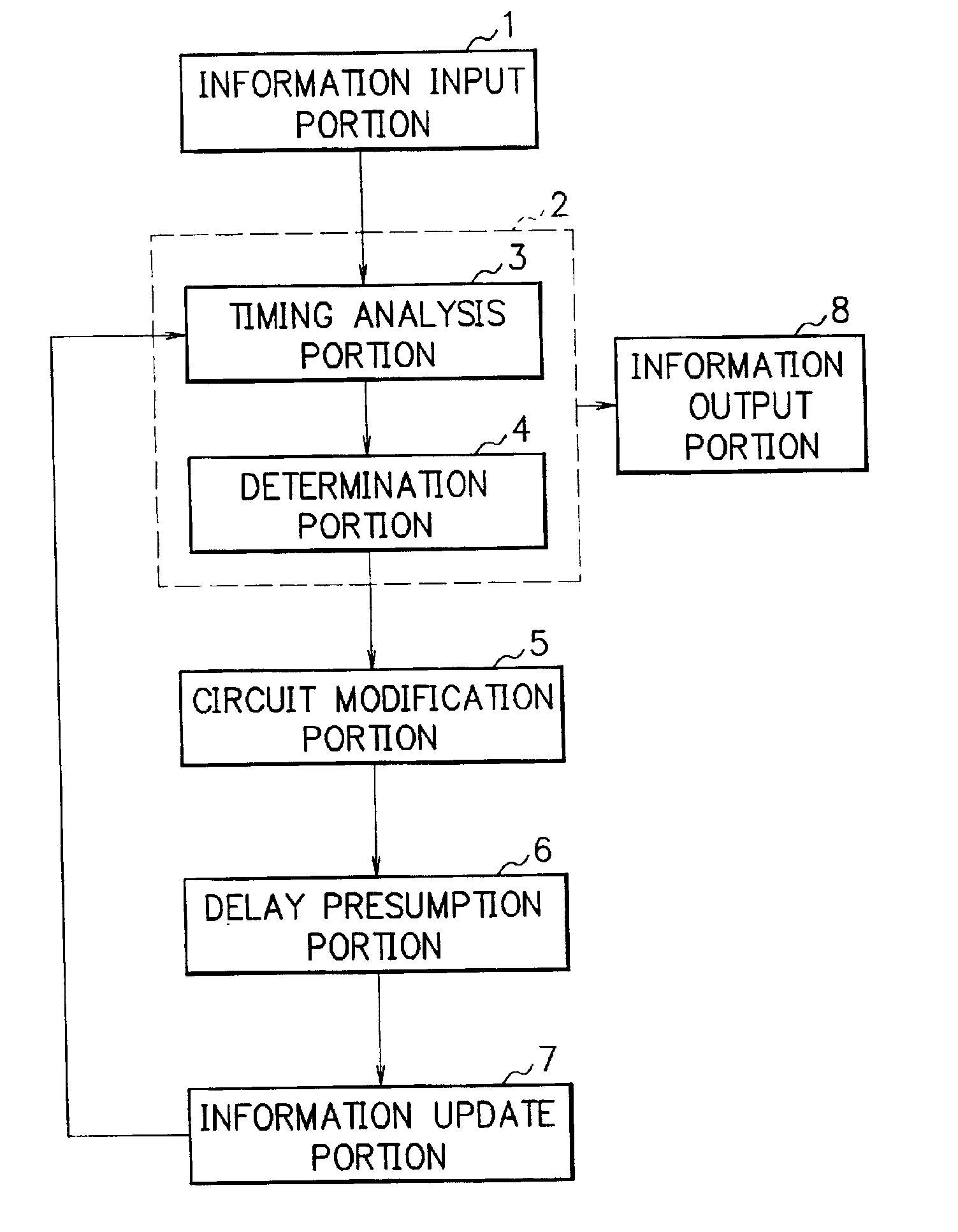
onfiguration to which applied is an integrated circuit design system related to the embodiment of the present invention;

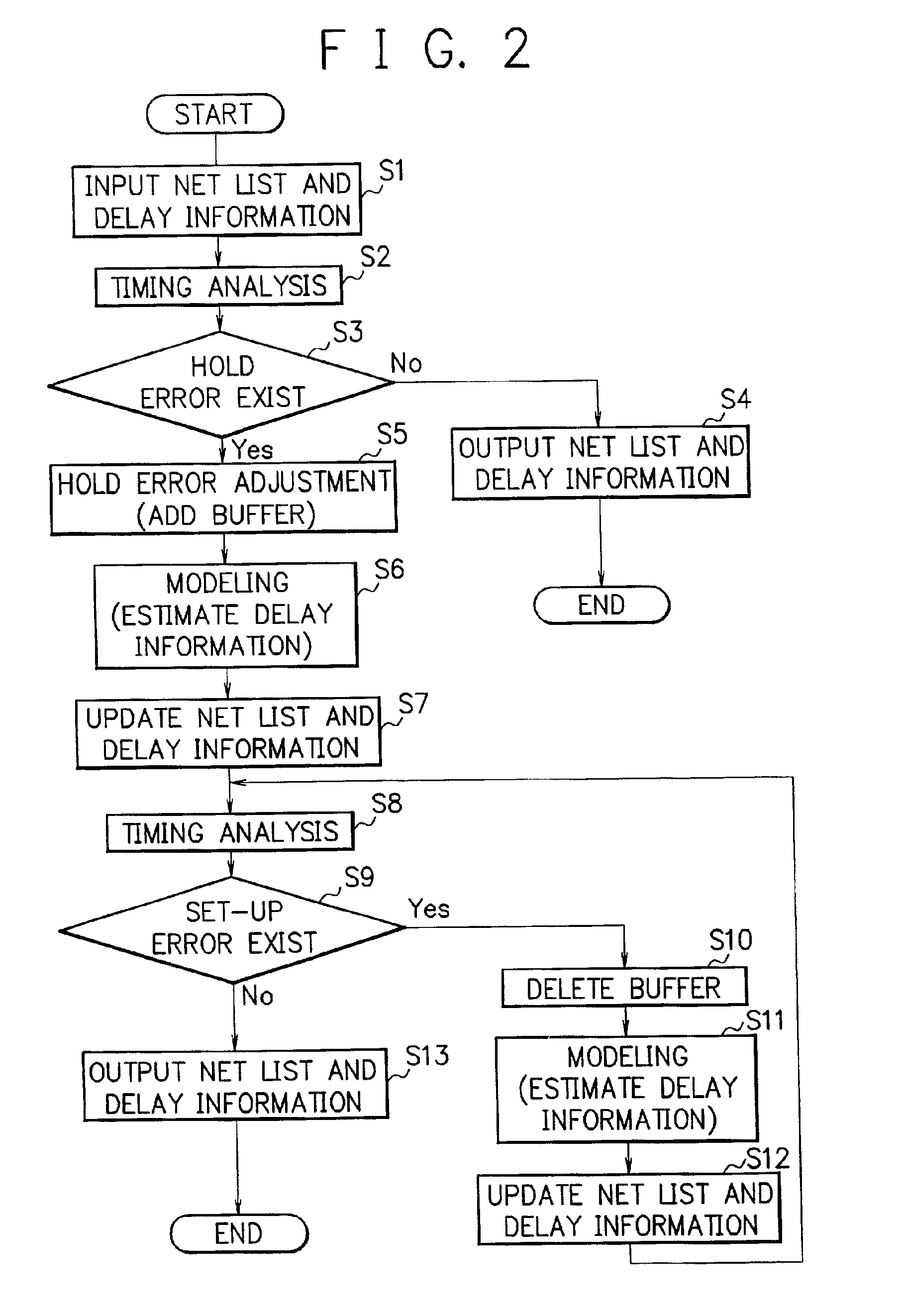
[0029]FIG. 2 is a flow chart showing the operation of the circuit design system related to this embodiment,

[0030]FIGS. 3A to 3D are diagrams showing one example of delay circuit models for estimating delay information,

[0031]FIG. 4 is a block diagram showing one example of a computer configuration achievable of the integrated circuit design system,

[0032]FIG. 5 is a circuit schematic view for describing a timing error, and

[0033]FIG. 6 is a timing chart showing one example of the circuit operation shown in FIG. 5.

DETAILED DESCRIPTION OF THE PREFERRED EMBODIMENTS

[0034]Details of an embodiment of the present invention will be explained based on the drawings.

[0035]FIG. 1 is a block diagram showing one example of a circuit design system configuration to which applied is an integrated circuit design system related to one embodiment of the present invention. The circuit des...


PUM


Abstract

A circuit modification portion modifies circuit information of an integrated circuit depending on a result of a timing test at a timing test portion to presume delay information at a delay presumption portion by modeling the circuit relating to its modified circuit information. Thereafter updating the circuit information and delay information of the integrated circuit at an information update portion to re-test the timing. This allows to carry out a timing analysis/test of the modified circuit without designing layout with the modified circuit information, which is required in a conventional design method. As a result, the number of designing the layout in the integrated circuit design is reduced to shorten time required for the layout design, which allows to shorten time required for the layout design process (layout design, timing analysis/test, and timing adjustment).

Description

CROSS-REFERENCE TO RELATED APPLICATIONS[0002]This application is based upon and claims priority of Japanese Patent Application No. 2001-291413, filed on Sep. 25, 2001, the contents being incorporated herein by reference.BACKGROUND OF THE INVENTION[0003]1. Field of the Invention[0004]The present invention relates to a design system of an integrated circuit and a design method and program of the integrated circuit and, more particularly, to the design system of the integrated circuit in order to analyze and adjust timing in the integrated circuit when designing the layout of the integrated circuit.[0005]2. Description of the Related Art[0006]In recent years, the layout design, which organizes the arrangement of respective circuit elements (e.g. logic gates) composing the integrated circuit on a chip and wiring between these circuit elements, has been complicated as the integrated circuit becomes large in scale and high-speed and the process becomes refined. The conventional layout des...

Claims


Application Information

Patent Timeline
IPC IPC(8): G06F17/50H01L21/82
CPCG06F17/5045G06F30/30
Inventor MATSUMOTO, SHO
Owner FUJITSU LTD
Why Eureka
Try Eureka