Output buffer with programmable voltage swing

a voltage swing and output buffer technology, applied in logic circuits, logic circuits, logic functions, etc., can solve the problems of unnecessary power consumption and heat generation, waste of 4 ma of current for each output y and yn

Inactive Publication Date: 2001-10-09
QUALCOMM INC
View PDF14 Cites 33 Cited by
  • Summary
  • Abstract
  • Description
  • Claims
  • Application Information

AI Technical Summary

Problems solved by technology

A significant shortcoming of prior art emitter coupled output circuits such as circuit 100 is that many applications do not require output voltage swings that are as large as the fixed output voltage swings provided, resulting in unnecessary power consumption and heat generation.
Thus, the outputs of the circuit 100 may provide 500 mV voltage swings to an application requiring only 300 mV voltage swings, resulting in 4 mA of current being wasted for each of the outputs Y and YN.
Although prior art circuits, such as those disclosed in U.S. Pat. No. 3,760,200 of Taniguchi et al., provide for reduction of fluctuations of the amplitude of circuit outputs, these circuits do not have a default operating mode where connection of an external resistor or current source is not required, and they consequently require connection of an external resistor or current source to the integrated circuit containing the output circuitry at all times.

Method used


Image

  • Output buffer with programmable voltage swing
  • Output buffer with programmable voltage swing
  • Output buffer with programmable voltage swing

Examples


embodiment 405

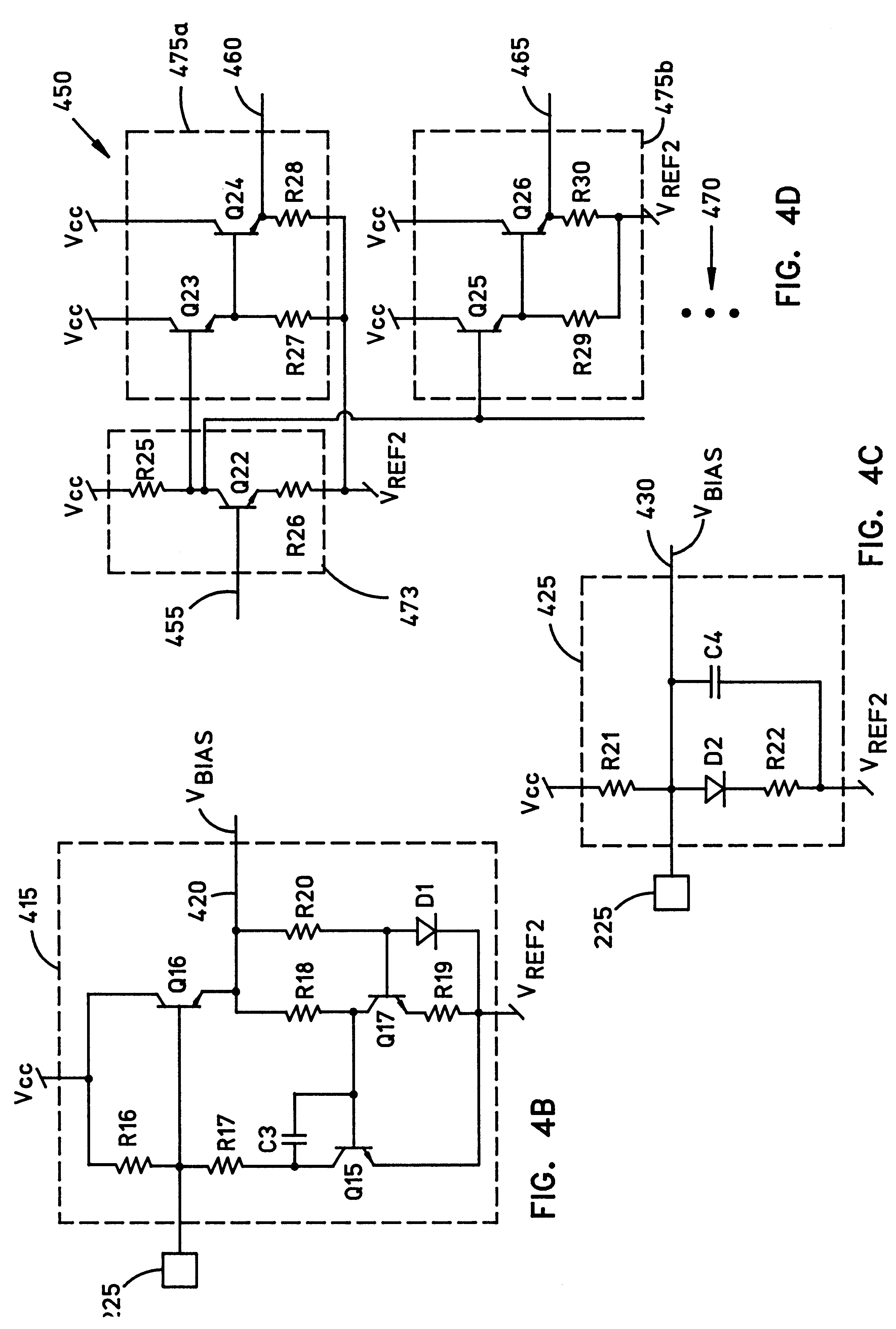
FIG. 4A illustrates a first alternative embodiment 405 of the variable bias generator 215 of FIG. 2. This alternative variable bias generator 405 includes a variable bias generator first resistor R13 that has a first end connected to the first reference voltage, and a second end connected to the electrical connection area 225. A variable bias generator second resistor R14 has a first end connected to the electrical connection area 225. A variable bias generator third resistor R15 has a first end connected to a second end of the variable bias generator second resistor R14. A variable bias generator first transistor Q11 has a collector connected to the electrical connection area 225, a base connected to the second end of the variable bias generator second resistor R14 and to the first end of the variable bias generator third resistor R15, and an emitter connected to a second end of the variable bias generator third resistor R15. A variable bias generator second transistor Q12 has a co...

embodiment 415

FIG. 4B illustrates a second alternative embodiment 415 of the variable bias generator 215 of FIG. 2. This alternative variable bias generator 415 includes a variable bias generator first resistor R16 that has a first end connected to the first reference voltage, and a second end connected to the electrical connection area 225. A variable bias generator second resistor R17 has a first end connected to the electrical connection area 225. A variable bias generator capacitor C3 has a first end connected to a second end of the variable bias generator second resistor R17. A variable bias generator first transistor Q15 has a collector connected to the first end of the variable bias generator capacitor C3 and to the second end of the variable bias generator second resistor R17, a base connected to a second end of the variable bias generator capacitor C3, and an emitter connected to the second reference voltage. A variable bias generator second transistor Q16 has a collector connected to th...

embodiment 425

FIG. 4C illustrates a third alternative embodiment 425 of the variable bias generator 215 of FIG. 2. This alternative variable bias generator 425 includes a variable bias generator first resistor R21 that has a first end connected to the first reference voltage, and a second end connected to the electrical connection area 225. A variable bias generator diode D2 has an anode connected to the electrical connection area 225, and a cathode. A variable bias generator second resistor R22 has a first end connected to the cathode of the variable bias generator diode, and a second end connected to the second reference voltage. A variable bias generator capacitor C4 has a first end connected to the electrical connection area 225, and a second end connected to the second reference voltage. An output 430 of the variable bias generator 425 is connected to the electrical connection area 225. The output 430 is for connection to the bias voltage inputs of the current sources Adof emitter coupled ou...


PUM


Abstract

An integrated circuit device in which the magnitude of the output voltage swings of outputs in a circuit having emitter coupled output transistors is programmable includes a variable bias generator that produces a bias voltage. The bias voltage is connected to the base of a current source transistor in order to program the magnitude of the output voltage swings. An electrical connection area of the integrated circuit device is connected to the bias voltage generator. An external programming circuit can be connected to the electrical connection area in order to set the bias voltage, to thereby program the desired magnitude of the output voltage swings. The external programming circuit typically can be a resistance or an external voltage source. The variable bias generator can be any of a number of circuits that produce a bias voltage that is dependent upon the external programming circuit connected to the electrical connection area, and that produce a default bias voltage if no external programming circuit is connected to the electrical connection area. Another aspect of the invention is a method for programming the magnitude of the output voltage swings in an integrated circuit device having emitter coupled output transistors. The invention provides the ability to program the magnitude of the output voltage swings of the outputs to increase the magnitude of the output voltage swings, or alternatively, to decrease the magnitude of the output voltage swings thereby advantageously saving power and preventing unnecessary heat generation.

Description

1. Field of the InventionThe invention relates to emitter coupled output circuits. More particularly, the invention concerns an integrated circuit having a pair of emitter coupled output transistors and an electrical connection area that is connectable to an external circuit to program the magnitude of the voltage swings of the outputs.2. Description of the Related ArtOutput buffers are common components of high speed logic circuits. FIG. 1 illustrates a typical prior art current mode logic (CML) output buffer circuit 100 that has emitter coupled outputs. In the buffer circuit 100, the emitters of output transistors Ql and Q2 are connected together, and are thus "emitter coupled." Resistor R1 is connected to the collector of transistor Q1, and resistor R2 is connected to the collector of transistor Q2. The collector of output transistor Q2 is connected to output Y, and the collector of output transistor Q1 is connected to complementary output YN. The output current 1101 for these em...

Claims


Application Information

Patent Timeline
Patent Type & Authority Patents(United States)
IPC IPC(8): H03K19/018
CPCH03K19/01837
Inventor SMETANA, KENNETH
Owner QUALCOMM INC
Why Eureka
Try Eureka