Apparatus and method for detecting faulty of cells in a semiconductor memory device

a technology of semiconductor memory and apparatus, applied in the direction of digital storage, electronic circuit testing, instruments, etc., can solve the problems of increasing the layout area of the tested chip, difficult to detect parametric faults or transients, and affecting the normal operation of the chip

Inactive Publication Date: 2001-10-09
SAMSUNG ELECTRONICS CO LTD
View PDF8 Cites 21 Cited by
  • Summary
  • Abstract
  • Description
  • Claims
  • Application Information

AI Technical Summary

Problems solved by technology

However, it is difficult to detect a parametric fault or a transient fault, which prohibit the normal operation of chips by affecting delay time, using the stuck-at fault model.
However, in the on-chip test, the layout area of the tested chip ...

Method used


Image

  • Apparatus and method for detecting faulty of cells in a semiconductor memory device
  • Apparatus and method for detecting faulty of cells in a semiconductor memory device
  • Apparatus and method for detecting faulty of cells in a semiconductor memory device

Examples


Embodiment Construction

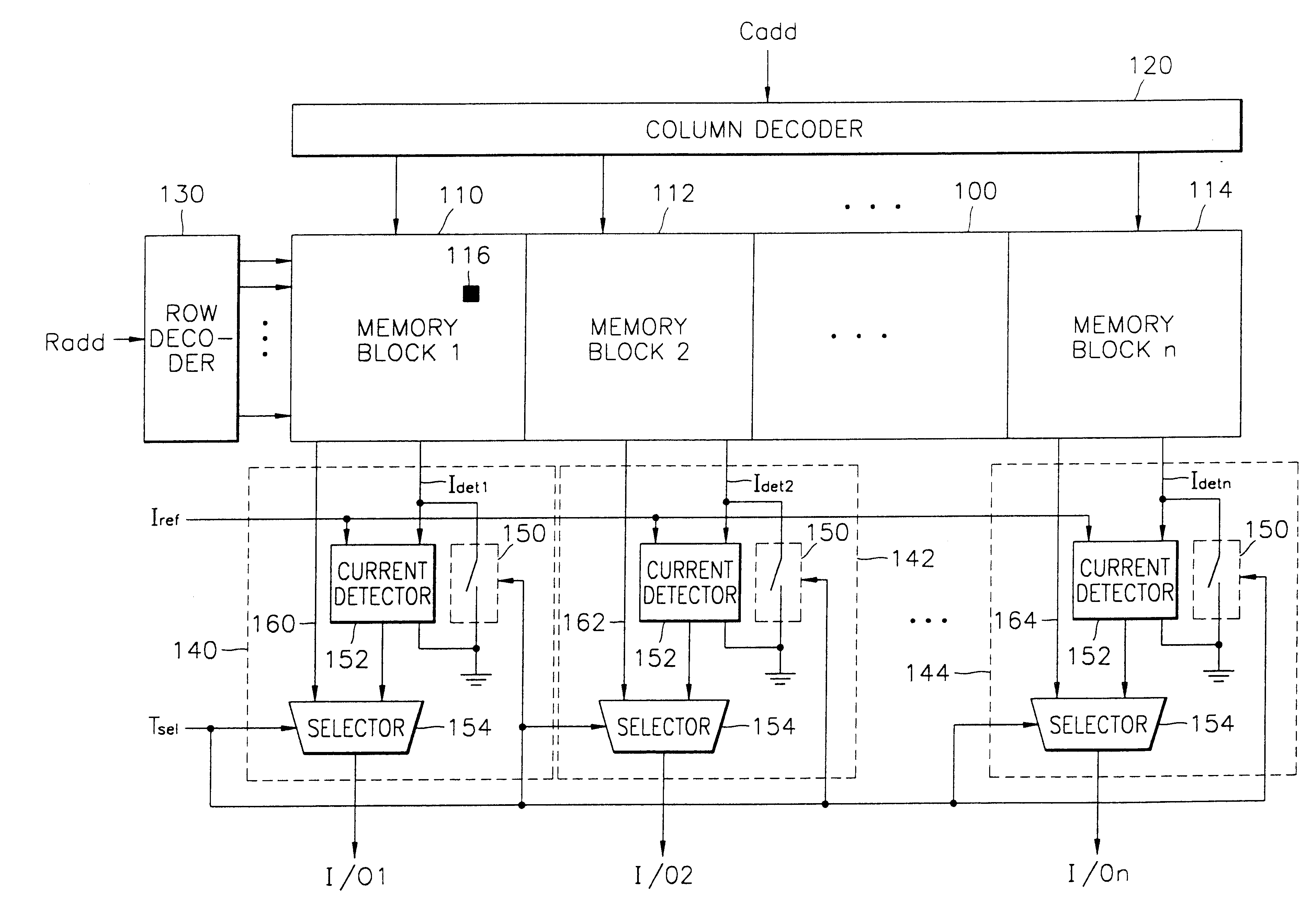
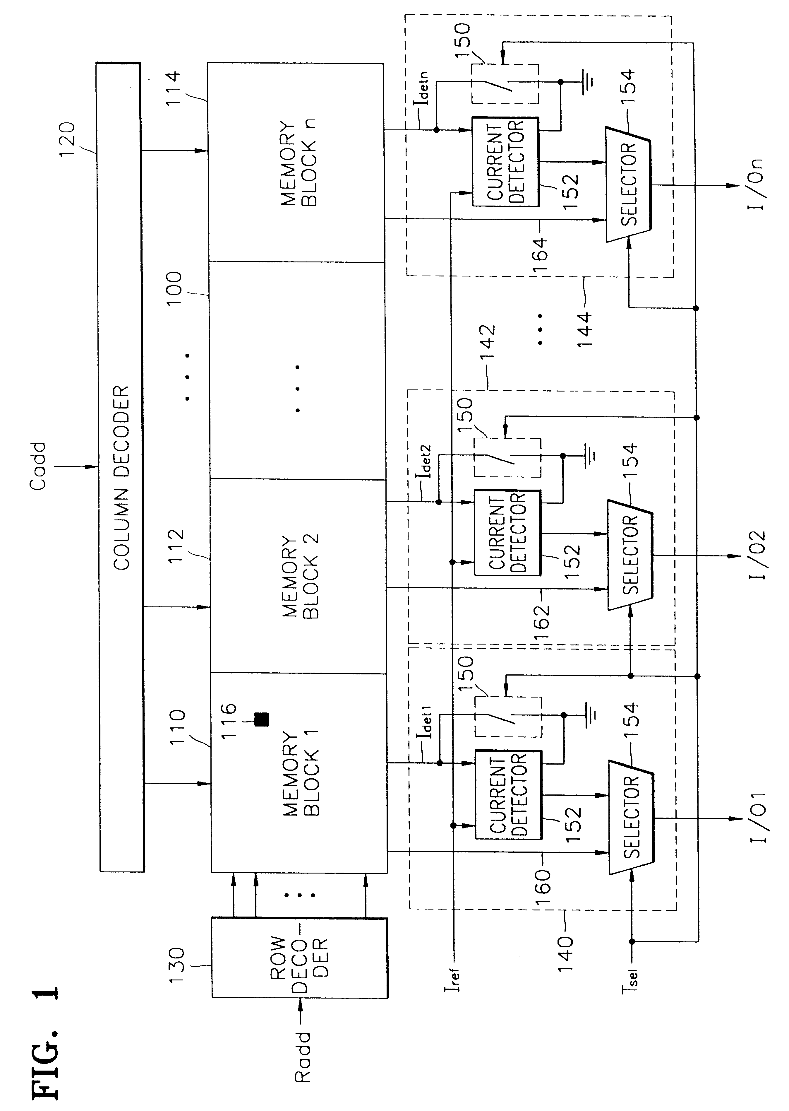
The present invention now will be described more fully with reference to the accompanying drawings, in which preferred embodiments of the invention are shown. FIG. 1 contains a schematic circuit diagram which shows an apparatus for detecting faulty cells in a semiconductor memory device according to an embodiment of the present invention. The apparatus for detecting faulty cells according to the present invention includes a memory cell array 100 which includes a plurality of memory blocks 110 through 114, a column decoder 120, a row decoder 130, and a plurality of faulty cell detectors 140 through 144.

Referring to FIG. 1, the memory cell array 100 includes the plurality of memory blocks 110 through 114. Each of the memory blocks 110 through 114 includes a plurality of memory cells 116. A memory cell is addressed in each of the memory blocks 110 through 114, corresponding to a predetermined memory address consisting of a column address Cadd and a row address Radd. That is, if the mem...


PUM


Abstract

A circuit and method for detecting faulty cells in a semiconductor memory device and a method therefor are provided. The circuit includes a memory cell array which includes a plurality of memory blocks, each of which includes a plurality of memory cells addressed corresponding to predetermined memory addresses and a plurality of faulty cell detectors corresponding to the plurality of memory blocks. The plurality of faulty cell detectors compare currents generated in the memory blocks to a predetermined reference current and detect whether addressed memory cells are faulty. It is possible to check whether the addressed memory cells are faulty by detecting the currents which flow through the plurality of memory blocks by the memory addresses. Therefore, it is possible to correctly detect the positions of faulty memory cells. Also, it is possible to reduce the number of pins since, data indicating whether the memory cells are faulty is output through data input and output lines in response to a test selection signal. Also, it is possible to prevent the operation speed of a chip from decreasing due to the current detectors during a normal operation since the current detectors corresponding to the memory blocks are bypassed in response to the test selection signal during the normal operation.

Description

1. Field of the InventionThe present invention relates to a semiconductor memory device, and more particularly, to an apparatus and a method for detecting faulty cells in a semiconductor memory device.2. Description of the Related ArtDue to the development of very large scale integration (VLSI) technology, the integration density and the operating speed of chips is increasing. Also, in order to reduce the area of chips, a narrow line width technology has been adopted. As a result, more cells can be integrated in the same chip area. Techniques for testing whether faults exist in chips have been a matter of concern as VLSI technology has developed.Various causes of faults in a VLSI circuit can be simply modeled. Among fault models of VLSI circuits, the most common one is a stuck-at fault model. Using the stuck-at fault model, it is possible to detect a logic operation fault, where the logic level of a node in the circuit is "stuck at" a logic "0" or "1". However, it is difficult to de...

Claims


Application Information

Patent Timeline
IPC IPC(8): G11C29/04G11C29/50G11C11/413G01R31/28G11C29/00G11C29/14
CPCG11C29/50G11C11/41G11C2029/5006G11C29/00
Inventor KIM, JIN-SUNG
Owner SAMSUNG ELECTRONICS CO LTD
Why Eureka
Try Eureka