Method for fabricating a type of trench mask ROM cell

a technology of mask rom and cell, which is applied in the direction of basic electric elements, electrical apparatus, semiconductor devices, etc., can solve the problems of increasing the performance of ics, more processing steps are needed to fabricate, and the type of mask rom cannot meet the reduction of the device scal

Inactive Publication Date: 2001-10-16
PROMOS TECH INC
View PDF4 Cites 143 Cited by
  • Summary
  • Abstract
  • Description
  • Claims
  • Application Information

AI Technical Summary

Problems solved by technology

As the complexity and performance of ICs increase, more processing steps are needed to fabricate them.
The typical planar type of Mask ROM can't satisfy the reductions for the device scale.
Hence, it is difficult to compose a huge number of devices on a small chip.
Furthermore, as the size of device is reduced, the distance between two adjacent components is so close as to cause the current leakage on the surface of the device.
Hence, the current leakage and small-scale integration lead the fabrication of the mask ROM to be restricted.

Method used


Image

  • Method for fabricating a type of trench mask ROM cell
  • Method for fabricating a type of trench mask ROM cell
  • Method for fabricating a type of trench mask ROM cell

Examples


Embodiment Construction

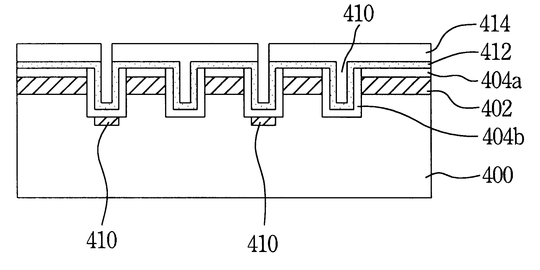
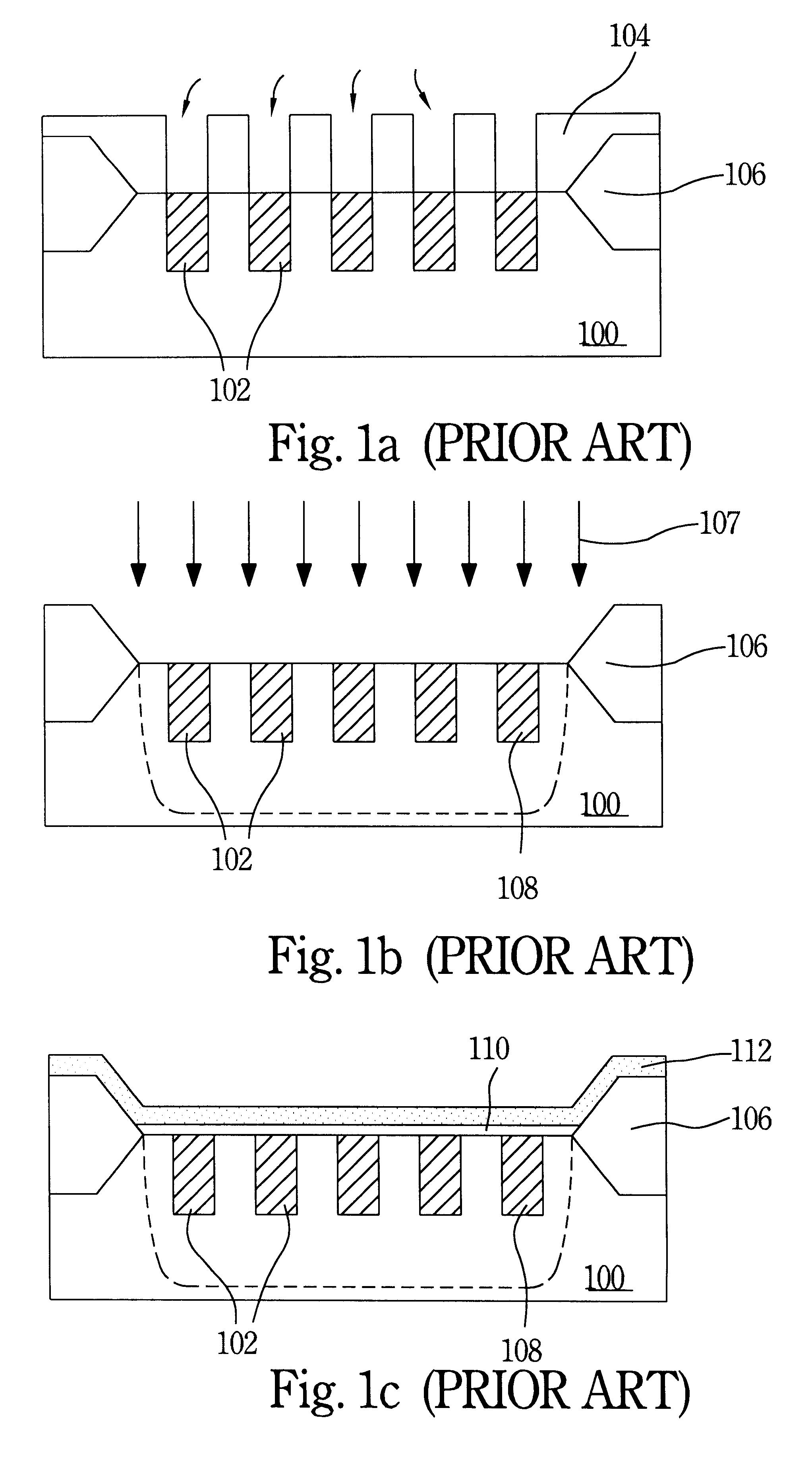
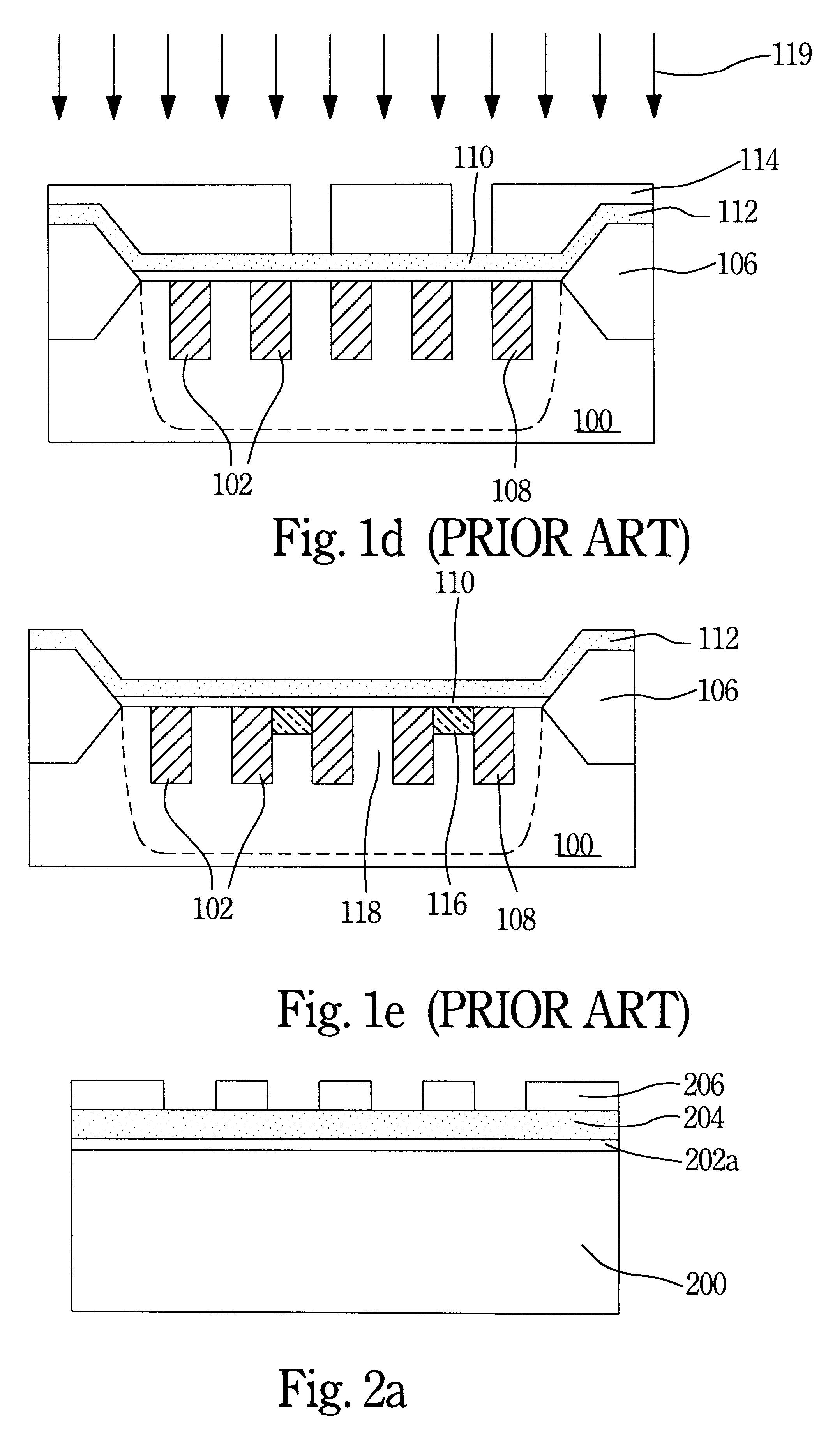
The following detailed description relates to a method for forming a new type of trench mask ROM cell in the present invention. Referring to FIG. 2a, a silicon substrate 200 is provided for fabricated devices. In the embodiment, the substrate 200 is preferably doped with a p-type dopant. A pad oxide layer 202a is formed on the substrate 200. The pad oxide layer 202a is composed of a silicon oxide using a process of thermal oxidization or deposition etc. In the embodiment, the thickness of the pad oxide layer 202a is about 300 to 600 angstroms. Then, a nitride layer 204 is formed on the pad oxide layer 202a. The nitride layer 204 is used to protect the oxide layer 202a during later etching steps. The nitride layer 204 has a thickness of about 1,000 to 2,000 angstroms. A photo resist 206 is formed on the nitride layer 204, wherein the photo resist 206 is used to define regions for etching to form plural trenches. Plural trenches 208, as shown in FIG. 2b are formed on the substrate 200...


PUM


Abstract

A method for fabricating a type of Trench Mask ROM cell comprises steps including: providing a substrate doped lightly with p-type dopant, sequentially forming a pad oxide layer and a nitride layer on the substrate; etching back the pad oxide layer, the nitride layer and the substrate to form plural trenches; a gate oxide layer being formed on surfaces of each trench; then, implanting n+-type ions into the substrate beneath the pad oxide layer and between each two adjacent trenches; and, forming a polysilicon layer on the gate oxide and pad oxide; finally, implanting n+-type ions into the substrate beneath the gate oxide layer on bottoms of selected trenches. And, it is appreciated that the sequence of the formation of plural trenches and implanting n+-type ions into substrate between each trench can be reversed in the embodiment without affecting subsequent steps.

Description

BACKGROUND OF INVENTION1. Field of the InventionThe present invention generally relates to a method of fabrication of a Mask ROM (Read Only Memory), and more precisely to a method of fabrication of a new type of Trench Mask ROM.2. Background of the Related ArtAs the complexity and performance of ICs increase, more processing steps are needed to fabricate them. Four or five mask levels were quite adequate for primitive ICs in the 1970s, whereas 16-Mb (ultra large-scale integration; ULSI) memory chips require more than twenty mask levels. For bit densities of up to one megabit, planar-type storage capacitors are used.Read Only Memory is so named because its cells can read data only from the memory cells. The ROM can be distinguished as Mask ROM, PROM (Programmable ROM), EPROM (Erasable Programmable ROM) and EEPROM (Electrically Erasable Programmable ROM) due to what method a ROM uses to store data. The Mask ROM is the most fundamental ROM.The fabrication of a typical planar type of Ma...

Claims


Application Information

Patent Timeline
Patent Type & Authority Patents(United States)
IPC IPC(8): H01L21/02H01L21/336H01L21/8246H01L27/112
CPCH01L27/112H01L27/11273Y10S438/923H10B20/40H10B20/00
Inventor SUNG, KUAN-CHOU
Owner PROMOS TECH INC
Why Eureka
Try Eureka