Built-in spare row and column replacement analysis system for embedded memories

a technology of embedded memory and analysis system, which is applied in the direction of electronic circuit testing, measurement devices, instruments, etc., can solve the problems of inability to use asic, inefficient use of spare column replacement system, and radiation damage to ram cells, etc., to achieve the effect of optimizing spare row and column allocation

Inactive Publication Date: 2001-10-16
CREDENCE SYSTEMS
View PDF9 Cites 78 Cited by
  • Summary
  • Abstract
  • Description
  • Claims
  • Application Information

AI Technical Summary

Benefits of technology

to provide a BIRA subsystem that can substantially optimize spare row and column allocation for an ASIC memory based on BIST subsyst

Problems solved by technology

However a RAM embedded in an ASIC may include thousands or millions of memory cells, and if any one of those cells is defective when manufactured, the ASIC is unusable.
Radiation can also damage RAM cells when an ASIC is in use.
Spare column replacement systems are not very efficient in their use of spare memory cells because they replace an entire column of memory cells even when only one cell in the column is defective.
Since such a bit map requires as many cells as the memory itself, it isn't practical to provide a circuit for storing and analyzing such a bit map on the ASIC itself.
For example radiation or other environmental factors can cause a memory cell in an ASIC to fail long after it has passed a test at the factory.
Self-contained BISR systems have not been able to take full advantage of the efficiencies provided by co

Method used


Image

  • Built-in spare row and column replacement analysis system for embedded memories
  • Built-in spare row and column replacement analysis system for embedded memories
  • Built-in spare row and column replacement analysis system for embedded memories

Examples


Embodiment Construction

BISR System Architecture

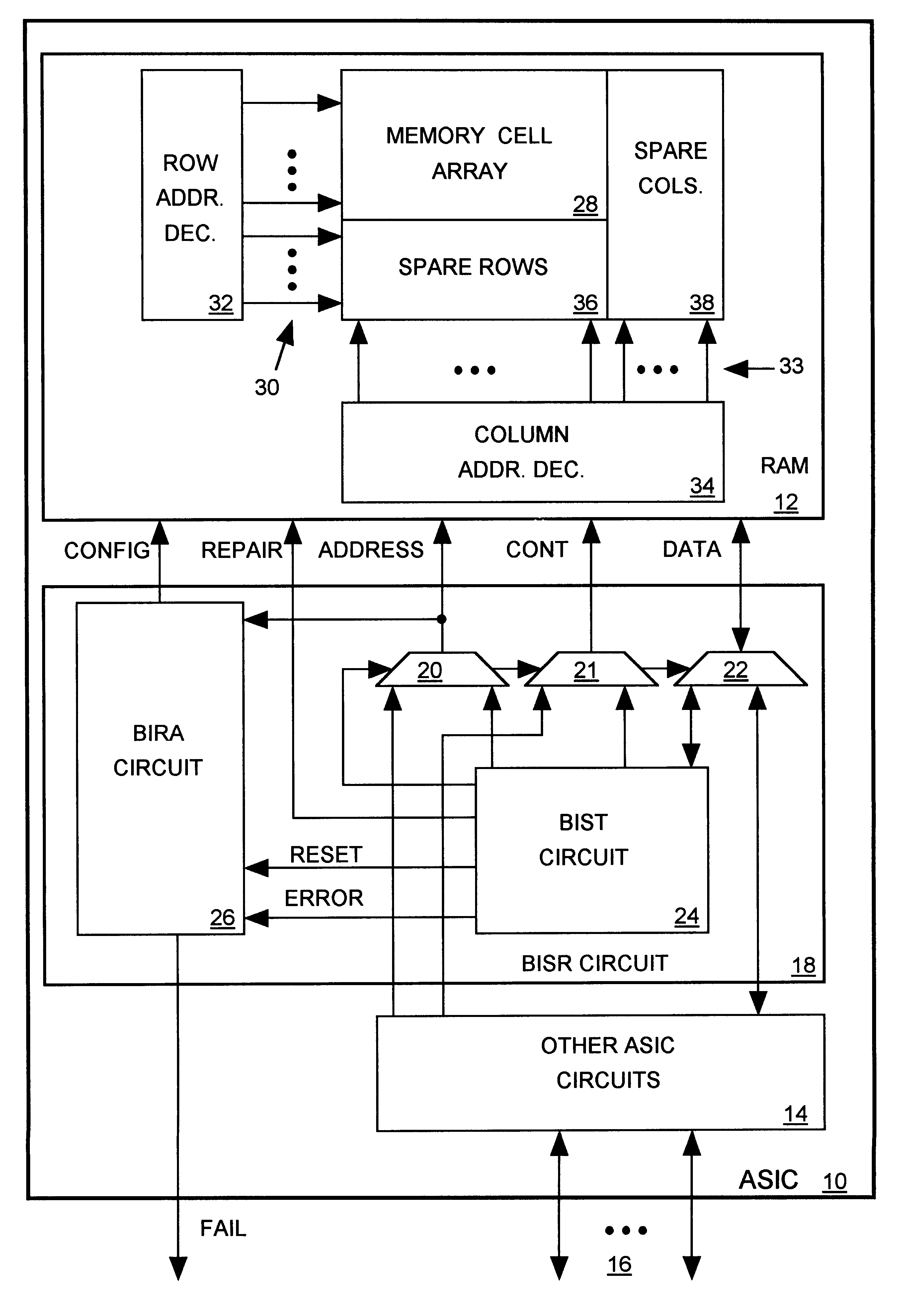
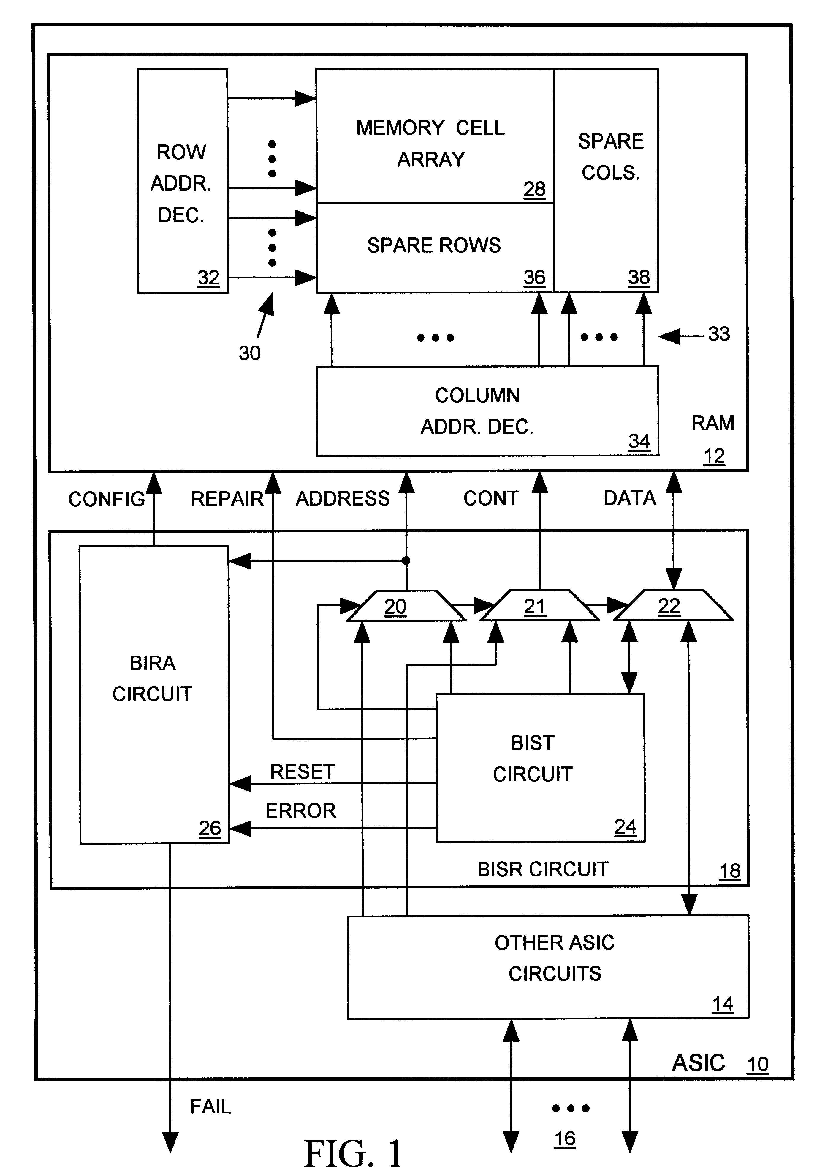
FIG. 1 illustrates in block diagram form an application specific integrated circuit (ASIC) 10 including an embedded random access memory (RAM) 12, and other ASIC circuits 14. During normal ASIC operation, ASIC circuits 14 also read and write access RAM 12 and communicate with external devices via the ASIC's input / output (I / O) terminals 16. Since the data, address and control terminals 32 of RAM 12 are not directly accessible to external test equipment via the ASIC's I / O terminals 16, a built-in self-repair (BISR) system 18 in accordance with the invention is incorporated into ASIC 10 to test and repair RAM 12.

ASIC circuits 14 normally read and write access the address, control and data terminals of RAM 12 via a set of multiplexers 20-22 included in BISR subsystem 18. However when BISR system 18 is to test RAM 12, (for example on system power up) a built-in self-test (BIST) subsystem 24 of BISR subsystem 18 switches multiplexers 20-22 to connect BIST subsystem...


PUM


Abstract

A built-in replacement analysis (BIRA) circuit allocates spare rows and columns of cells for replacing rows and columns of an array of memory cells in response to an input sequence of cell addresses, each identifying a row address and a column address of each defective cell of the cell array. The BIRA subsystem, including a row register corresponding each spare row and a column register corresponding to each spare column, responds to incoming cell addresses by writing their included row address into the row registers, by writing their column addresses into the column registers, and by writing link bits into the column registers. Each link bit links a row and a column register by storing row and column addresses of a defective cell. The BIRA subsystem also writes a "multiple cell" bit into each row register to indicate when the row address it stores includes more than one defective cell. The row and column addresses stored in these registers indicate the array rows and columns for which spare rows and columns are to be allocated. Each row and column register also includes a "permanent" bit the BIRA subsystem sets to indicate when the spare row or column allocation indicated by its stored row or column address is permanent. The BIRA subsystem efficiently allocates spare row and columns by manipulating the data stored in the row and column registers in response to a sequence of defective cell address.

Description

1. Field of the InventionThe present invention relates in general to built-in self-repair (BISR) systems for integrated circuits employing embedded memories, and in particular to a BISR system employing an efficient spare row and column replacement analysis system.2. Description of Related ArtIntegrated circuit (IC) designers often incorporate one or more random access memories (RAMs) into application specific integrated circuits (ASICs) to avoid manufacturing and performance costs associated with interconnecting the ASICs to separate RAMs at the circuit board level. However a RAM embedded in an ASIC may include thousands or millions of memory cells, and if any one of those cells is defective when manufactured, the ASIC is unusable. Radiation can also damage RAM cells when an ASIC is in use.One approach to decreasing the percentage of ASICS that are unusable due to defective memory cells has been to replace defective memory cells with spare cells that have been incorporated into the...

Claims


Application Information

Patent Timeline
IPC IPC(8): G11C29/00G01R31/28G11C29/02G11C29/04G11C29/12G11C29/44
CPCG11C29/44G11C29/4401G11C29/72G11C29/00
Inventor KRAUS, LAWRENCEBATINIC, IVAN-PIERRE
Owner CREDENCE SYSTEMS
Why Eureka
Try Eureka