

Surface acoustic wave device and method for fabricating the same
a surface acoustic wave and acoustic wave technology, applied in piezoelectric/electrostrictive devices, piezoelectric/electrostrictive/magnetostrictive devices, semiconductor devices, etc., can solve the problems of pushed up manufacturing costs of surface acoustic wave devices, and the inability to secure a hollow portion over the surface of functional portions 1a
- Summary
- Abstract
- Description
- Claims
- Application Information
AI Technical Summary
Problems solved by technology
Method used
Image

Examples
embodiment 1
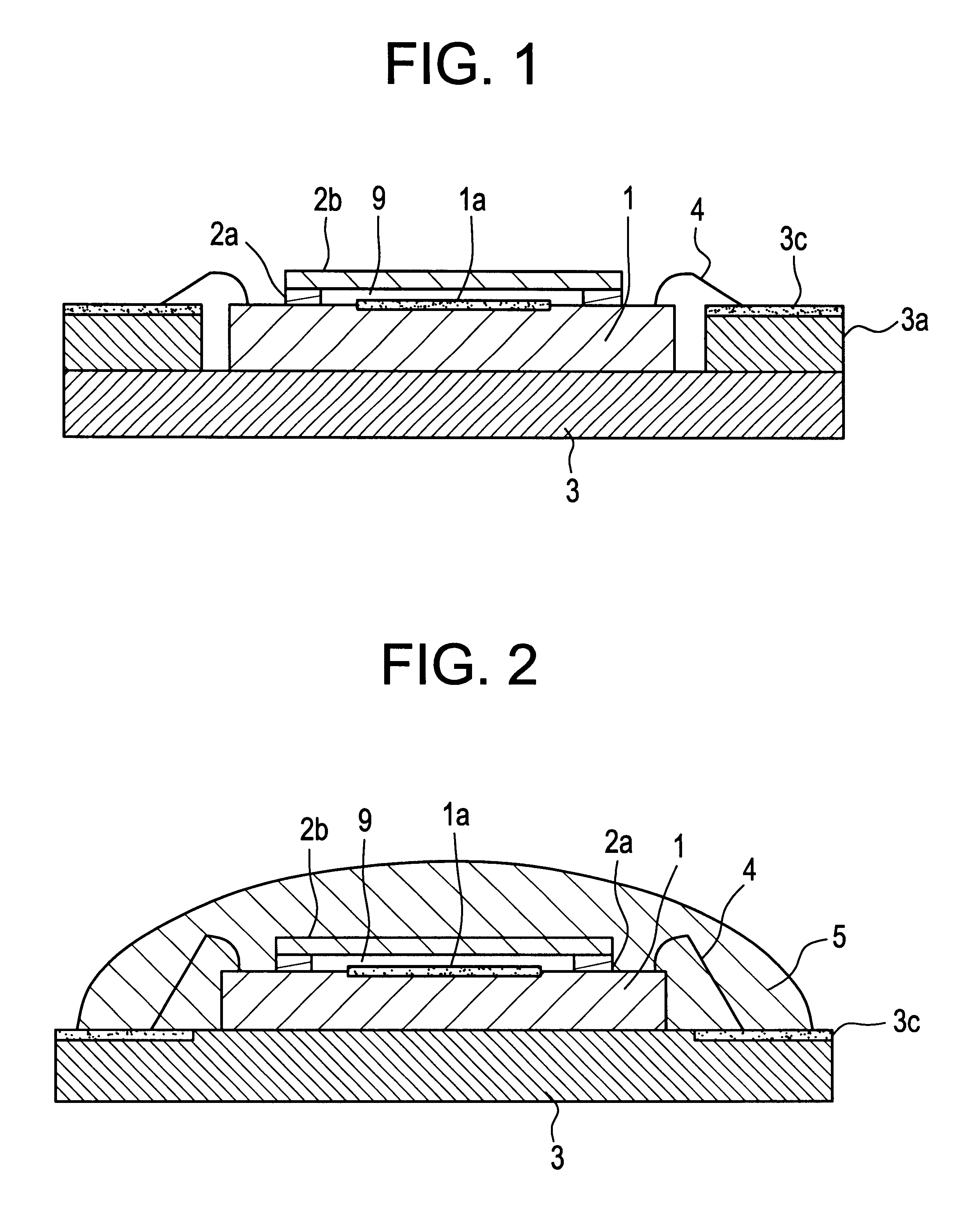
this invention will now be described with reference to FIG. 1. FIG. 1 is a cross-sectional view of a surface acoustic wave device according to embodiment 1.
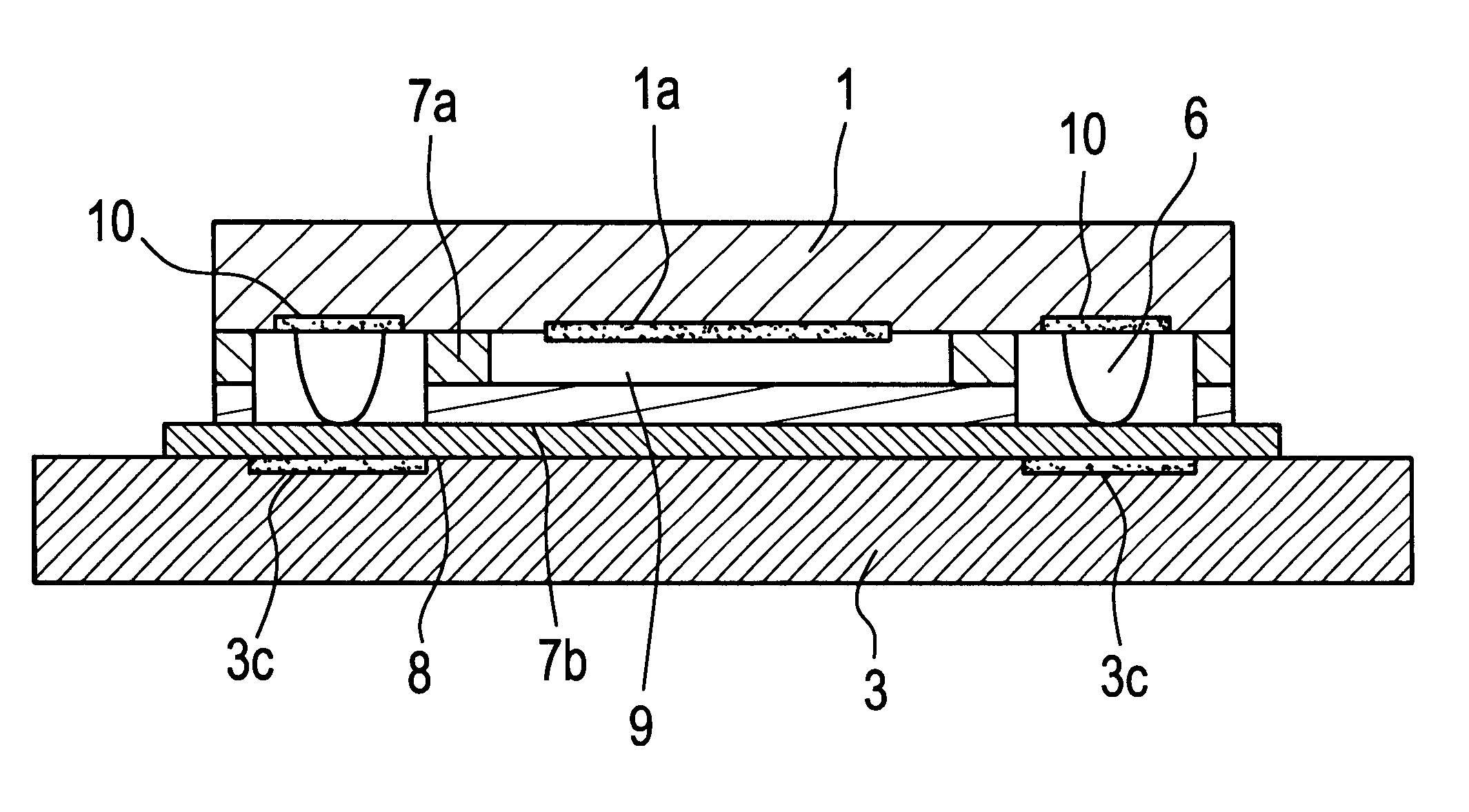
In FIG. 1, reference numeral 1 denotes a piezoelectric substrate chip constituting a surface acoustic wave element. On a principal plane of the chip 1 (upper surface in FIG. 1) are a surface acoustic wave functional portion 1a and electrode pads (not shown). The functional portion 1a comprises driving electrodes made of known IDTs, and propagation paths for surface waves driven in a predetermined direction on the chip surface. The electrode pads, extend from the driving electrodes and serve as external connection terminals of the functional portion 1a.
Reference numeral 3 denotes a circuit substrate on which to mount the chip; 3c for a terminal portion formed on a part of the circuit substrate 3; 4 for wires that connect the electrode pads of the functional portion 1a electrically to the terminal portion 3c; 2a for a frame-like fi...
embodiment 2
An embodiment 2 of the invention will now be described with reference to FIG. 2. FIG. 2 is a cross-sectional view of a surface acoustic wave device according to embodiment 2. In FIG. 2, those parts with their counterparts already shown in FIG. 1 are given the same reference numerals, and descriptions of such parts are omitted where they are repetitive.
In FIG. 2, reference numeral 5 represents an insulating resin. The chip 1, with its functional portion 1a capped by the first and the second insulating film 2a and 2b, is mounted on the circuit substrate 3. Metal wires 4 are used to connect the functional portion 1a electrically to the terminal portion 3c. The insulating resin 5 is deposited so as to cover the chip 1 and metal wires 4. This makeup ensures the same effects as the embodiment 1 and provides a surface acoustic wave device still more reliable than the embodiment 1.
embodiment 3
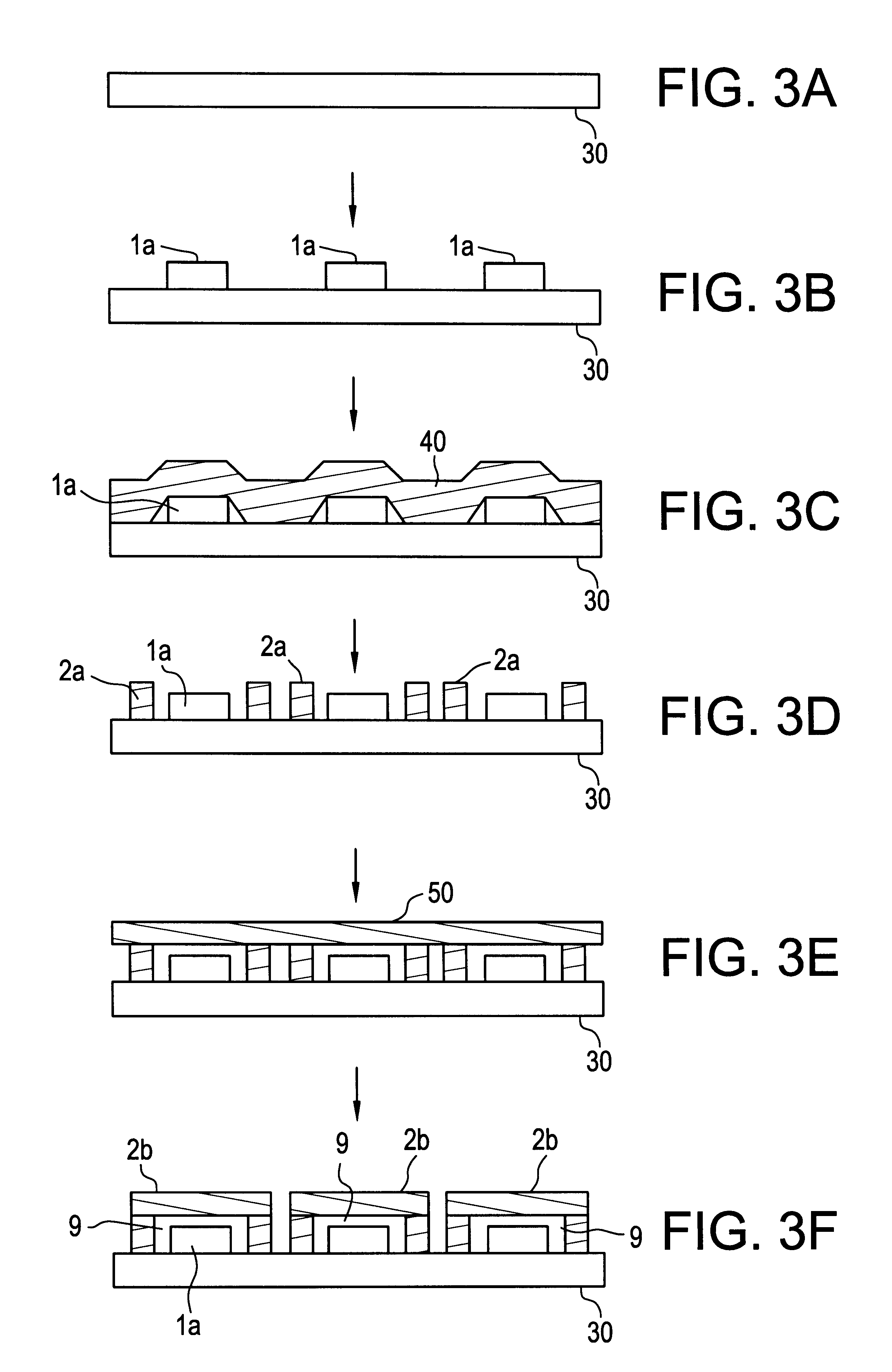
An embodiment 3 of this invention will now be described with reference to FIGS. 3A to 3F, and FIGS. 4A and 4B. FIGS. 3A to 3F are schematic views showing steps to fabricate a chip for use by a surface acoustic wave device according to the embodiment 3. FIGS. 4A and 4B are perspective views illustrating respectively typical states of the chips in FIGS. 3D and 3F as they are being fabricated.
FIG. 3A shows a wafer 30. On the wafer 30, a plurality of functional portions 1a are formed through conductor patterning at suitable intervals as indicated in FIG. 3B.
A photosensitive film 40 is then deposited on all functional portions 1a on the wafer 30 as illustrated in FIG. 3C. With the film 40 in place, a frame-like first insulating film 2a is formed by photolithography so as to surround each functional portion as shown in FIGS. 3D and 4A. FIG. 4A depicts a case in which two functional portions 1a are surrounded by the first insulating film 2a.
Thereafter, a single photosensitive film 50 is de...
PUM
 Abstract
Description
Claims
Application Information