Self cleaning method of forming deep trenches in silicon substrates

a deep trench and self-cleaning technology, applied in the direction of hollow article cleaning, solid-state devices, chemistry apparatus and processes, etc., can solve the problems of increasing the number of process gases required to control, introducing complexities, and reducing deposits

Inactive Publication Date: 2001-11-20
APPLIED MATERIALS INC
View PDF9 Cites 89 Cited by
  • Summary
  • Abstract
  • Description
  • Claims
  • Application Information

AI Technical Summary

Problems solved by technology

However, these methods of deposit reduction may have adverse impacts on the trench process.
The addition of self-clean chemistry, while reducing accumulations, increases the number of process gases required to control and introduces complexities in the interactions between the various trench etch gases and the self-clean gases.
Turning off SiF.sub.4 during the last 90 seconds of the trench etch may also negatively impact the hard mask layer since the SiF.sub.4 reduces lateral erosion.
As decreased device size leads to deeper trenches, the longer trench etch times needed for these deeper trenches increases the risk of lateral erosion.

Method used


Image

  • Self cleaning method of forming deep trenches in silicon substrates
  • Self cleaning method of forming deep trenches in silicon substrates
  • Self cleaning method of forming deep trenches in silicon substrates

Examples


Embodiment Construction

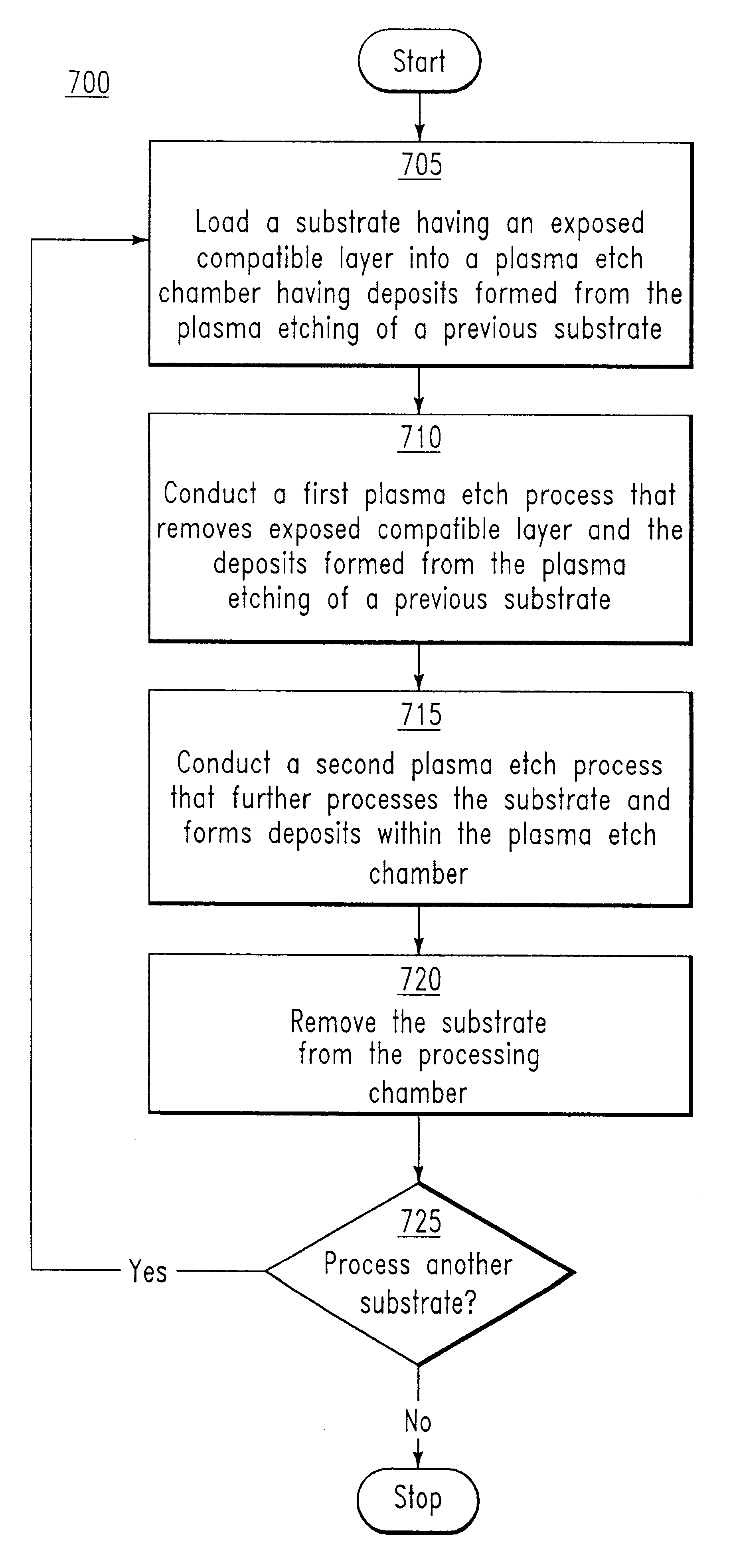
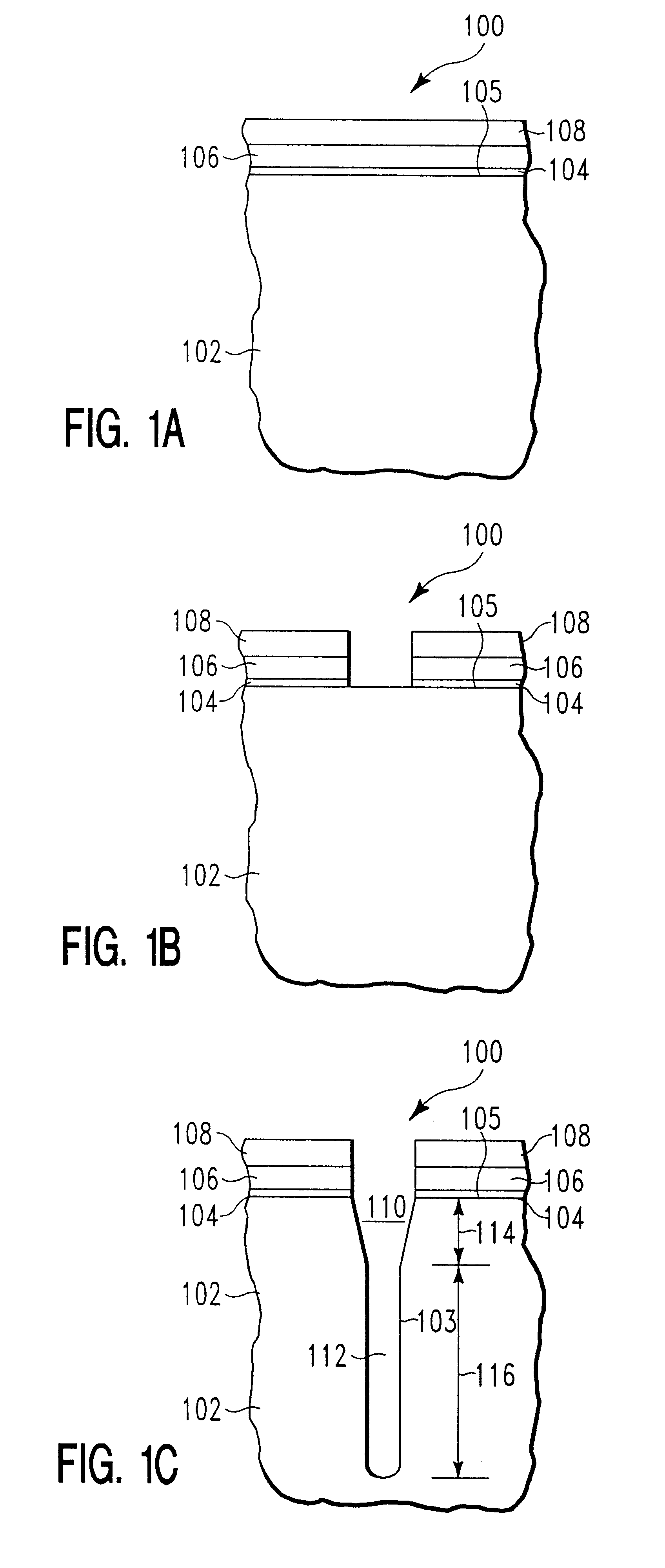
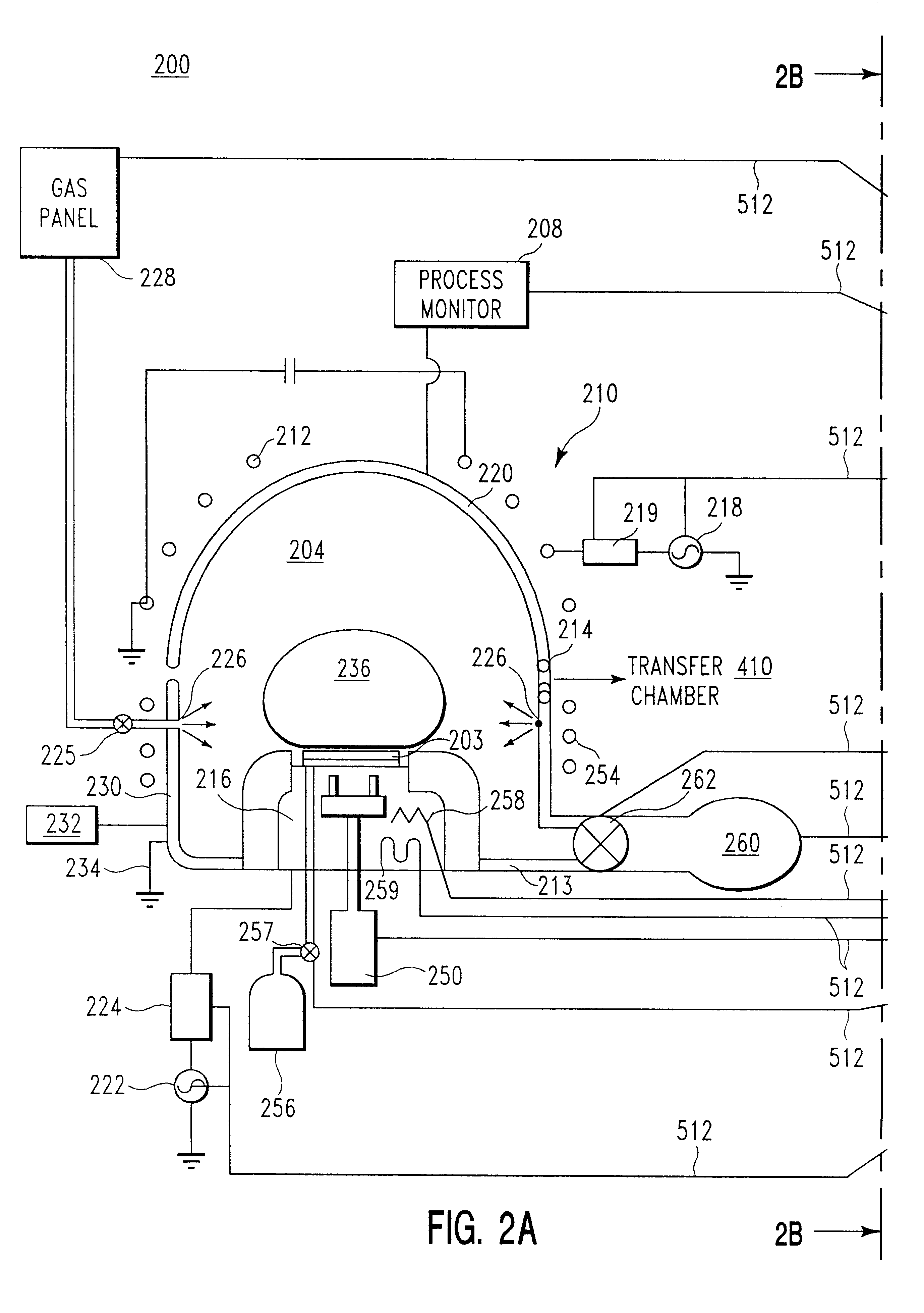
The method of the present invention can be implemented on a processing system having a single processing chamber. While any of a variety of processing chambers may enjoy the advantages of the present invention, the method will be described as implemented on a computer controlled HDP etching chamber 200 as illustrated and described below in FIG. 2. The present invention provides a method to etch a layer or one of a plurality the layers formed on a substrate while simultaneously removing deposits formed within the chamber from a previously processed substrate. In an embodiment of the present invention, the layer to be etched is compatible with the deposits formed within the chamber. Advantageously, processing efficiencies are realized since a single step is utilized to process a substrate while cleaning the deposits produced by processing the previous substrate. In this way, etching a layer on one substrate is combined with cleaning the residue formed from etching a previous substrate...


PUM

PropertyMeasurementUnit
diameteraaaaaaaaaa
diameteraaaaaaaaaa
critical diameteraaaaaaaaaa

Abstract

This invention is directed to a method for etching films on semiconductor substrates and cleaning etch chambers. The method includes an improved processing sequence and cleaning method where residue formed from processing a previous substrate are cleaned by the etching process used to remove an exposed layer of material from the present substrate. The process provides improved substrate throughput by combining the step to clean residue from a previous substrate with an etch step conducted on the present substrate. Applicants have found the method particularly useful in processing structures such as DRAM stacks, especially where the residue is formed by a trench etched in the previous silicon substrate and the exposed layer etched from the present substrate is silicon nitride.

Description

1. Field of the InventionThe present invention pertains to etching trenches in silicon substrates and cleaning processes to remove deposits from reactors used in etching processes. The method of the invention is generally applicable to the etching of silicon, but is particularly useful in the etching of deep trenches. Silicon deep trench etching is most commonly used in capacitor technology, in particular, in DRAM applications. Other applications for the present etching method include the etching of shallow trenches used in applications such as device isolation; the etching of polysilicon gates; and the etching of silicide layers. In addition, the present etching method is useful in process sequences utilized in the micro machining of silicon surfaces for biomedical applications, for example.2. Description of the Related ArtAlthough the silicon etching method of the present invention is useful in a number of applications, as mentioned above, one of the most important applications is...

Claims


Application Information

Patent Timeline
Patent Type & Authority Patents(United States)
IPC IPC(8): H01L21/70H01L21/762H01L21/02H01L21/00H01L21/3065H01L21/8242
CPCH01L21/3065H01L21/67069H01L21/76232H01L27/1087Y10S156/916H10B12/0387
Inventor KHAN, ANISULKUMARCHINN, JEFFREY D.PODLESNIK, DRAGAN
Owner APPLIED MATERIALS INC
Why Eureka
Try Eureka