Method for manufacturing a thermoelectric semiconductor material or element and method for manufacturing a thermoelectric module

a manufacturing method and semiconductor technology, applied in semiconductor devices, instruments, heat measurement, etc., can solve the problems of insufficient durability as a thermoelectric element, the inability to achieve the expected level of thermoelectric performance, and the inability to use a single crystal as a thermoelectric material with the single crystal unchanged

Inactive Publication Date: 2001-11-20
KOMATSU LTD
View PDF5 Cites 51 Cited by
  • Summary
  • Abstract
  • Description
  • Claims
  • Application Information

AI Technical Summary

Problems solved by technology

However, when the characteristics of the thermoelectric element actually manufactured by the above-described method were examined, the expected level of thermoelectric performance was not obtained.
However, in the stratified-structure compound described above, because the bonding forces between the layers are weaker than the bonding forces within the layer surfaces, its use as a thermoelectric material with the single crystal unchanged is undesirable in terms of the material strength.
By way of example, because, in a Bismuth-Tellenium-based stratified-structure compound, weak van Der Waal's bonds exist between the Tellenium atoms, it has marked cleavage properties, and in a state which is close to single crystal, its durability as a thermoelectric element is inadequate.
It is thought that the thermoelectric performance does not improve as expected in conventional methods because the process is completed at this stage.
It is thought that this is attributable to the fact that the grains crushed in the laminated interface 18 are difficult to grow in the direction in which the pressure is imparted.

Method used


Image

  • Method for manufacturing a thermoelectric semiconductor material or element and method for manufacturing a thermoelectric module
  • Method for manufacturing a thermoelectric semiconductor material or element and method for manufacturing a thermoelectric module
  • Method for manufacturing a thermoelectric semiconductor material or element and method for manufacturing a thermoelectric module

Examples


Embodiment Construction

)

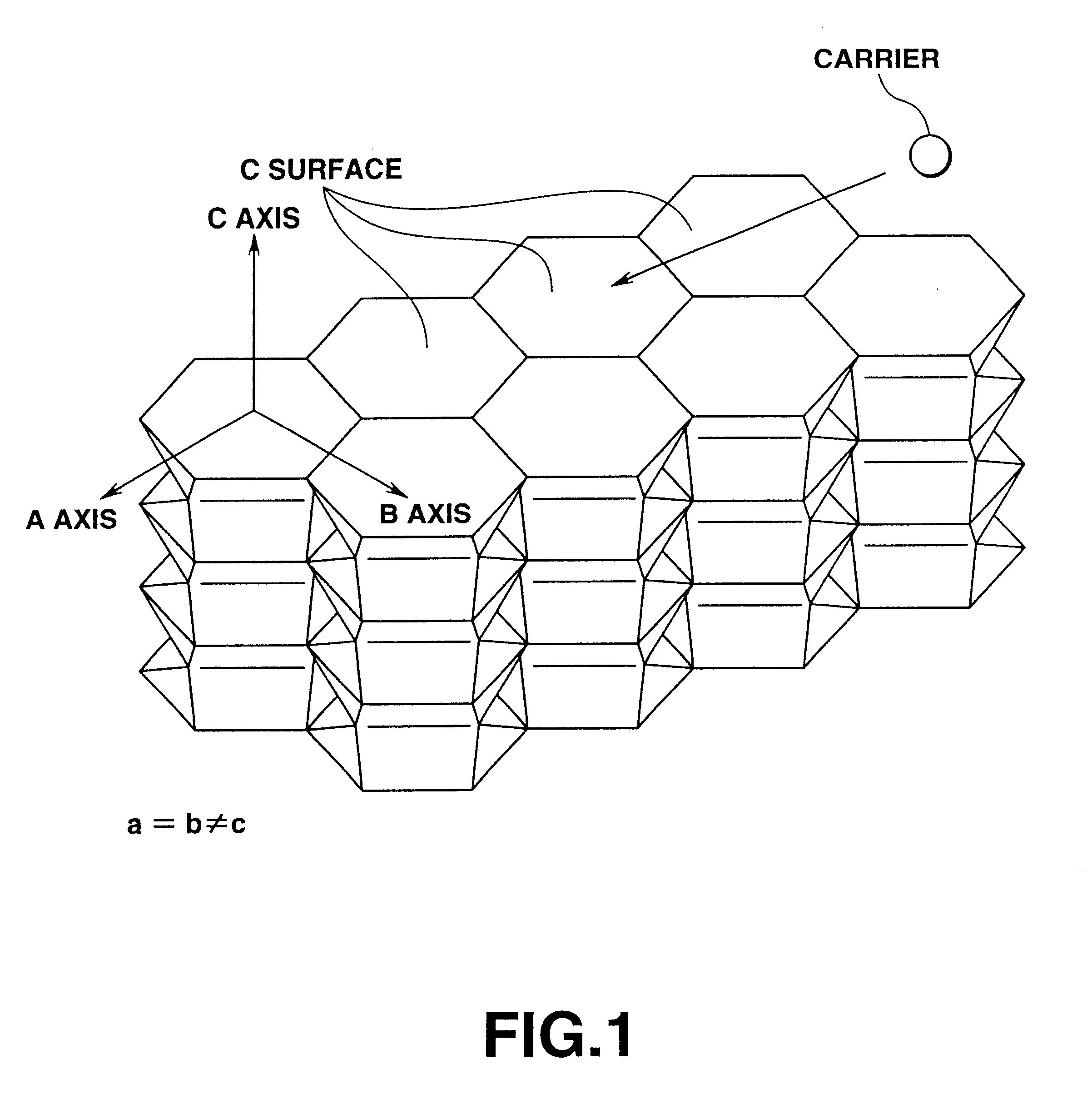
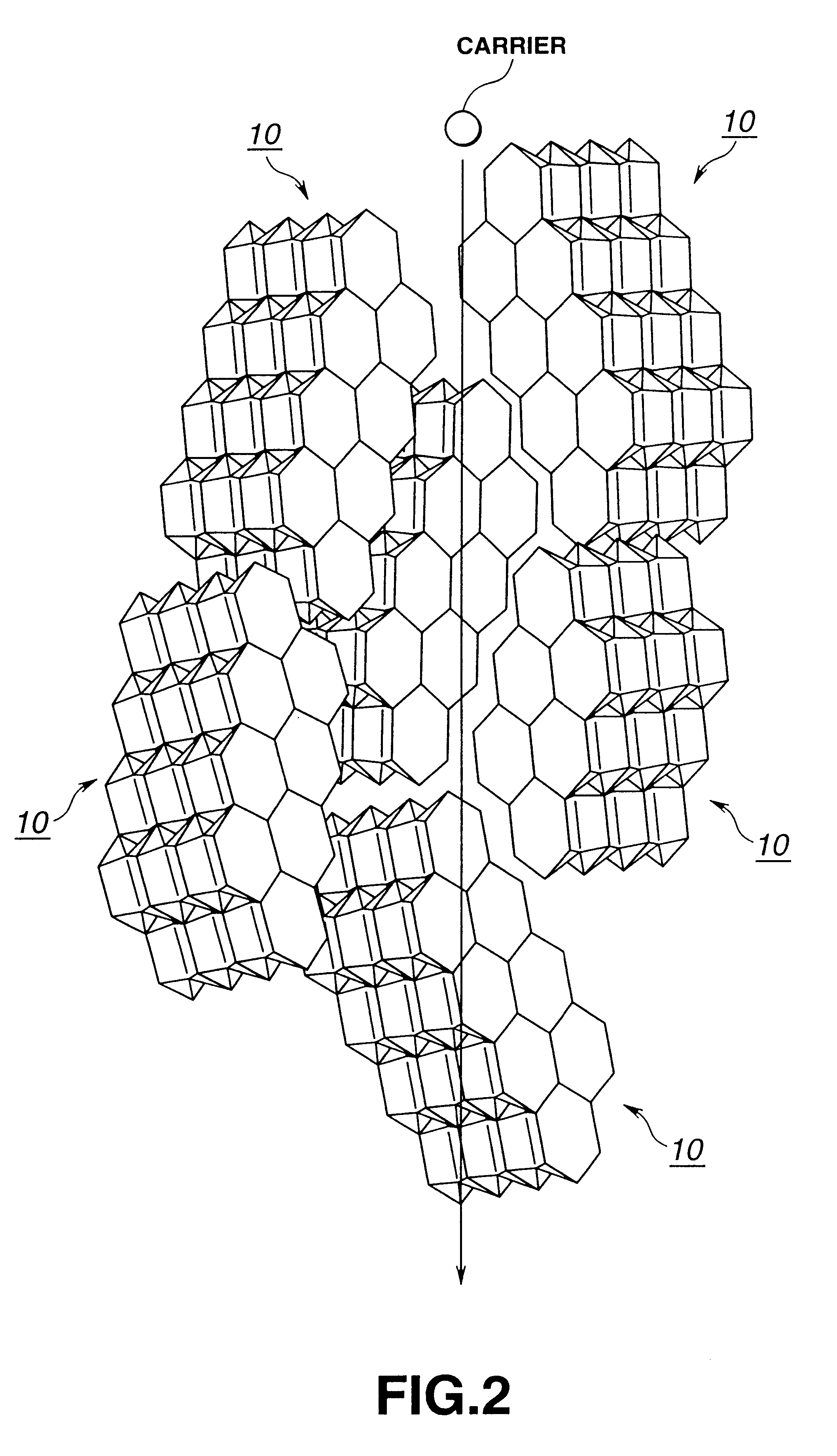
The technical concept described above, in which the crushing and the disturbance of the grains generated by the vertical compression P1 are repaired, is an idea which is extremely effective in terms of its improvement of the thermoelectric performance. Here, the technical concept having this feature is shown in a concrete example using a mode that is considered desirable from the viewpoint of industrial application. It will be noted that, among the elements of the configuration described above, and in particular of those for which an additional description is not thought to be necessary, the same names and same reference symbols have been attached and the detailed description thereof omitted. In addition, the embodiment shown below represents a concrete example of the present invention, but the present invention is not limited to this.

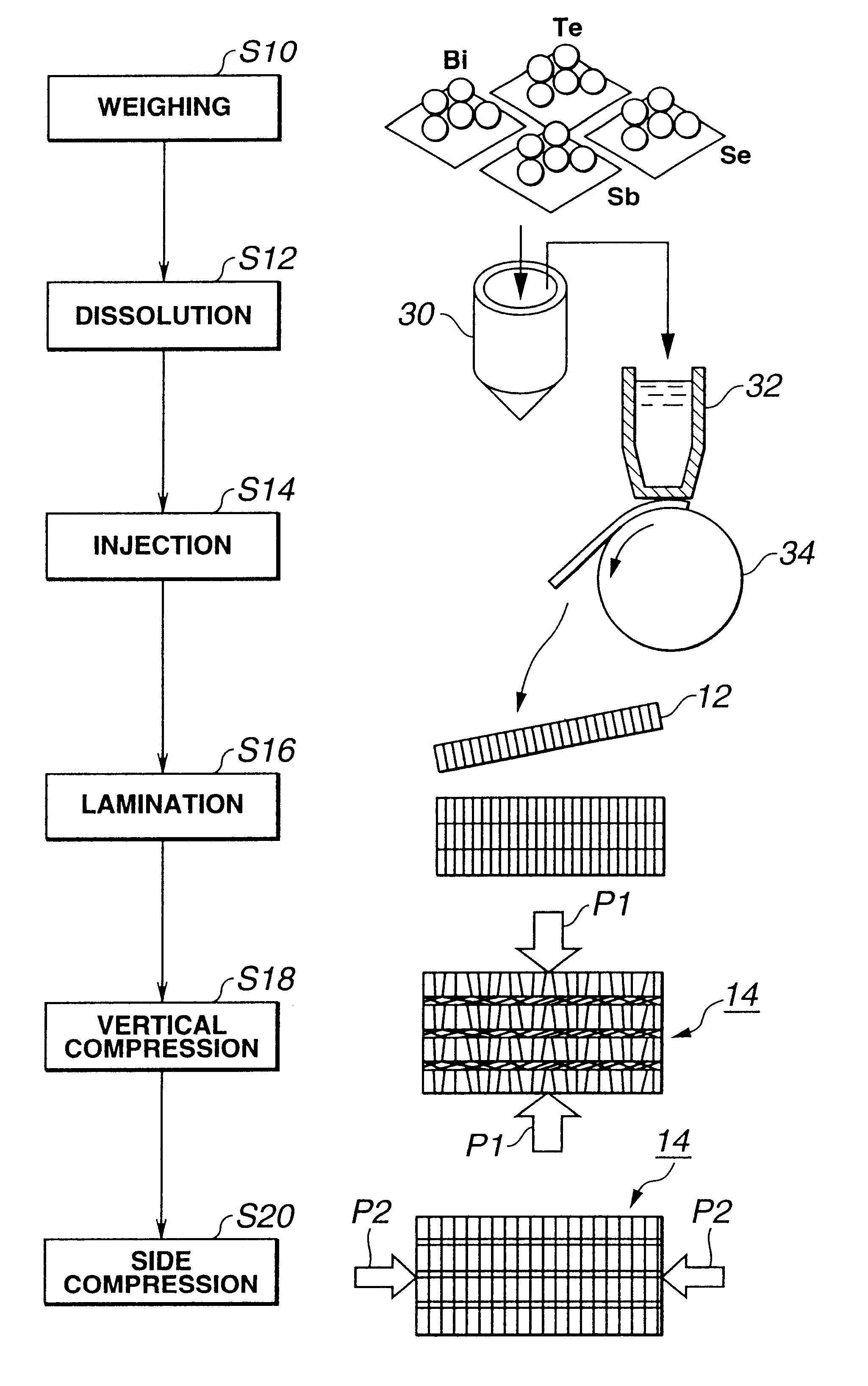
FIG. 8 is a flow chart which shows the entire configuration of the manufacturing process of the thermoelectric elements pertaining to the present emb...


PUM

PropertyMeasurementUnit
thicknessaaaaaaaaaa
diameteraaaaaaaaaa
diameteraaaaaaaaaa

Abstract

To provide a method for manufacturing a thermoelectric semiconductor material or a thermoelectric semiconductor element and method for manufacturing a thermoelectric module effective in improving thermoelectric performance. The thermoelectric semiconductor material is manufactured by producing a laminated body of thin powders manufactured by a quenching roller method, and compressing simultaneously the side surfaces of the laminated body using a secondary punch.

Description

1. Field of the InventionThe present invention relates to a method for manufacturing a thermoelectric semiconductor material or element and a method for manufacturing a thermoelectric module, and more particularly, it relates to a method for manufacturing a thermoelectric semiconductor material or element and a method for manufacturing a thermoelectric module effective in improving thermoelectric performance.2. Description of the Related ArtHitherto, thermoelectric elements that utilize thermoelectric phenomena have been employed as heat exchangers and temperature sensors. These thermoelectric phenomena are commonly known as the Peltier effect, Thomson effect and Seebeck effect, a description of each of which is given below.The Peltier effect is a phenomenon arising when an electric current flows to the junction between different metal types and heat is generated or absorbed at the junction, and the Thomson effect is a phenomenon arising when an electric current flows to a metal whi...

Claims


Application Information

Patent Timeline
Patent Type & Authority Patents(United States)
IPC IPC(8): G01K7/02
CPCG01K7/02Y10S438/965
Inventor HOON, LEE YONGKAJIURA, TAKEJI
Owner KOMATSU LTD
Why Eureka
Try Eureka