Liquid crystal device and process for production thereof

a technology of liquid crystal and liquid crystal, which is applied in the direction of static indicating devices, instruments, non-linear optics, etc., can solve the problems of low-quality picture giving a rough appearance as a whole, increasing production costs, and difficulty

Inactive Publication Date: 2001-11-20
CANON KK
View PDF39 Cites 32 Cited by
  • Summary
  • Abstract
  • Description
  • Claims
  • Application Information

AI Technical Summary

Problems solved by technology

The presence of such mixture domains 81a and 81b in an outside-pixel region 80c is liable to result in a low-quality picture giving a rough appearance as a whole.
This difficulty is also encountered in case where a bistable chiral nematic liquid crystal is subjected to multiplexing drive.
If the masking layer is formed as a metal film, the formation and photolithographic steps for patterning thereof incur an increase in production cost.
Further, it is well known that a liquid crystal device using a bistable liquid crystal is rather vulnerable to an impact, and the fixation of the substrates for alleviating the difficulty is also liable to incur a production cost increase.
Further, as the liquid crystal device is further enlarged in area, it becomes difficult to retain a uniform cell gap in a central region of the device by holding substrates llaa and llbb to each other only at their peripheries, so that it has been also practice to dis

Method used


Image

  • Liquid crystal device and process for production thereof
  • Liquid crystal device and process for production thereof
  • Liquid crystal device and process for production thereof

Examples


example 2

A chiral nematic liquid crystal device was prepared in the following manner.

Two substrates 2a and 2b were treated in the same manner as in Example 1 up to the formation of the color filters 4, the vertical structure 7 at the outside-pixel region 8a and the transparent electrodes 5. Then, each substrate was coated with a polyimide alignment film 6 ("SE-3140", available from Nissan Kagaku K.K.), followed by rubbing.

The thus-treated two substrates 2a and 2b were then applied to each other with spacer beads dispersed therein so as to provide a gap of 2 .mu.m therebetween and so that their rubbing directions were parallel and opposite to each other.

Separately, a chiral nematic liquid crystal 3 having a helical H pitch of 3.4 .mu.m was prepared by adding an optical dopant to a nematic liquid crystal composition ("KN-400", available from Chisso K.K.) and injected into the gap between the substrates 2a and 2b to form a liquid crystal device.

As a result of multiplexing drive, the liquid crys...

second embodiment

Next, a liquid crystal device according to the present invention will be described.
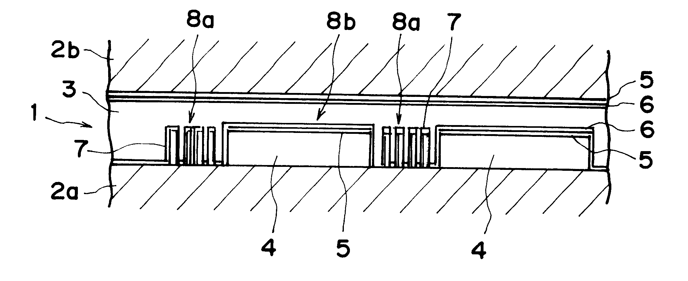
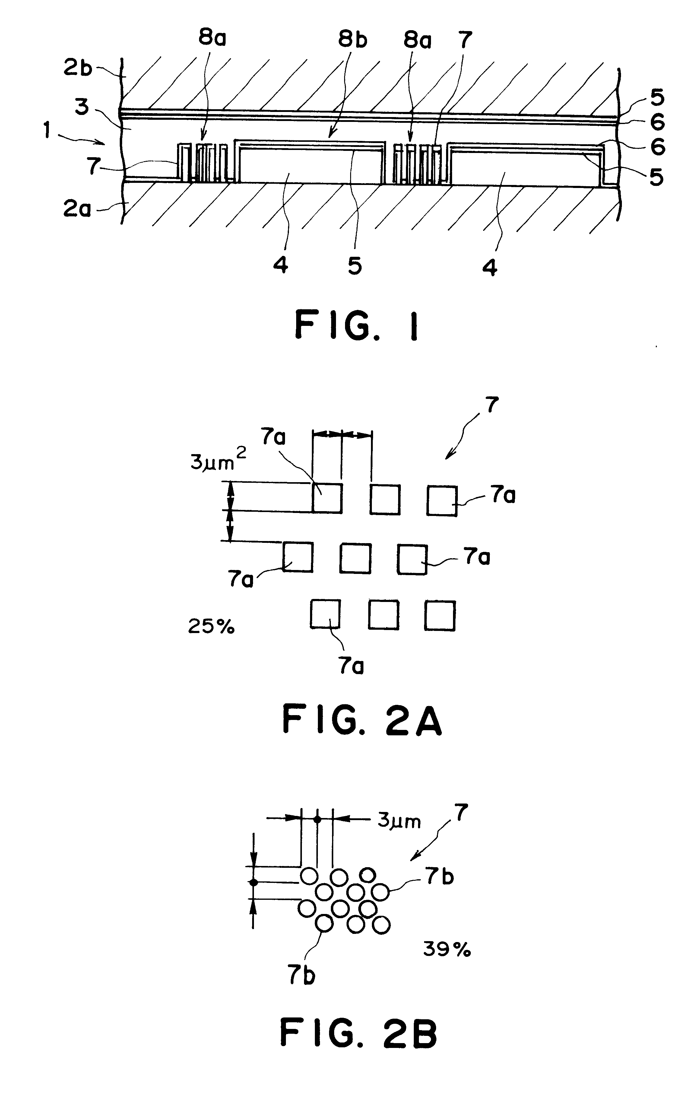
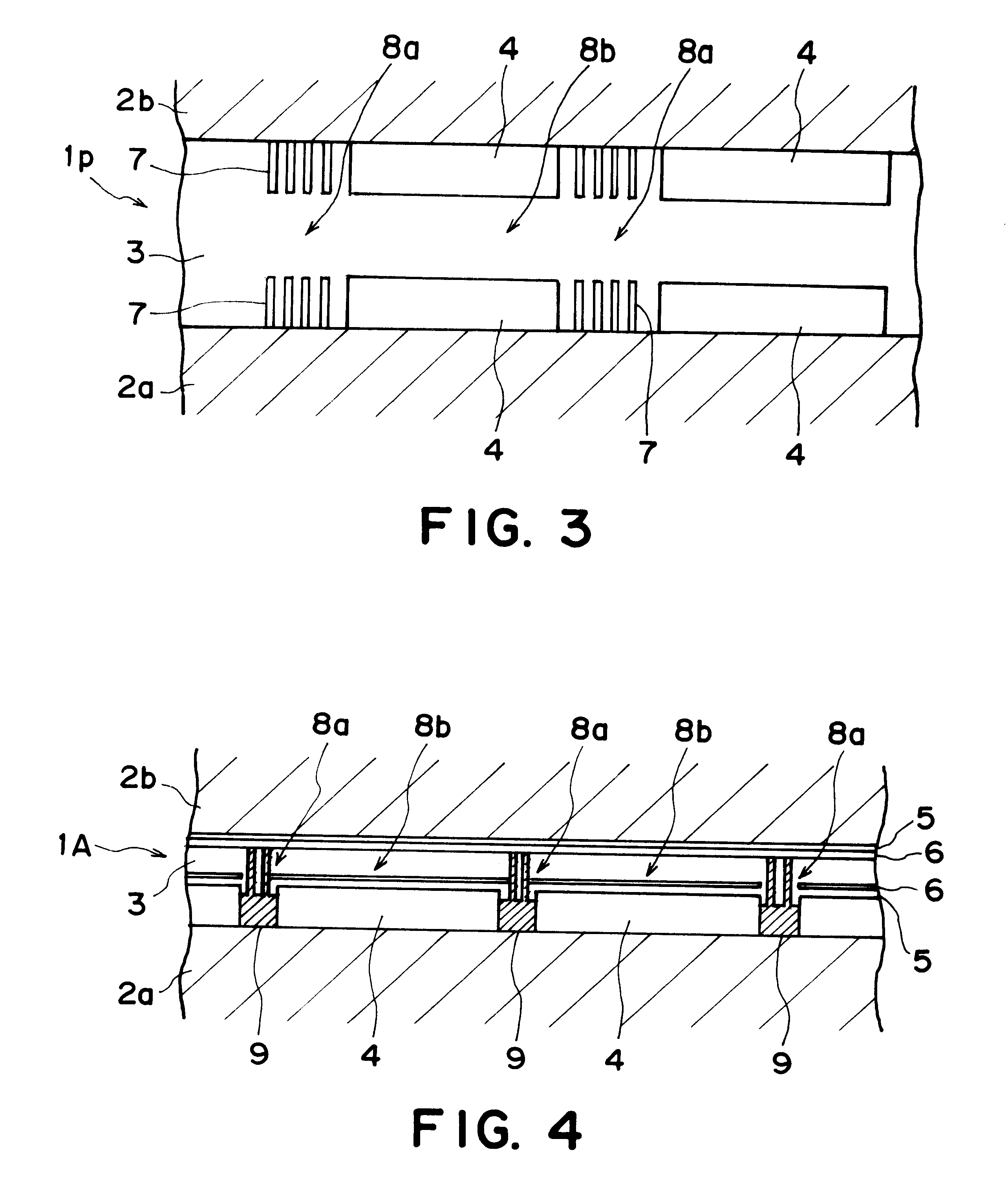
first embodiment

Referring to FIG. 3, a liquid crystal device 1p according to this embodiment includes color filters 4 and vertical structures 7 on both substrates 2a and 2b. Each color filter may have a thickness of, e.g., 0.75 .mu.m (about a half that of the color filter 4 in the first embodiment), and color filters 4 at opposing positions on both substrates may have an identical color.

The liquid crystal device 1p may be prepared by forming the color filter 4 and vertical structure 7 on each of the substrates 2a and 2b and thereafter performing formation of electrodes and alignment film, rubbing and application of the substrates similarly as in the first embodiment. Incidentally, it is possible to omit the color filters 4 from one substrate, e.g., 2b, while forming only the vertical structure 7 on the substrate 2b.


PUM


Abstract

A matrix-type liquid crystal device is formed so as to have a matrix of pixels defined by and isolated from each other by an outside-pixel region. The liquid crystal in the outside-pixel region in placed in an alignment state, typically a homeotropic state or one close thereto, which is different from an alignment state, typically a homogeneous uniform alignment state, at the pixel region. As a result, the liquid crystal device is provided with improved display qualities due to suppression of irregularities at the outside-pixel region and/or a local pressure distribution.

Description

FIELD OF THE INVENTION AND RELATED ARTThe present invention relates to a liquid crystal device having a pixel region and an outside-pixel region providing different liquid crystal alignment states allowing improved performances and a process for production thereof, particularly such a liquid crystal device using a liquid crystal having bistability, such as a chiral smectic liquid crystal, and a process for production thereof.A liquid crystal device of a type which controls transmission of light by utilizing the refractive index anisotropy of liquid crystal molecules in combination with a polarizing device has been proposed by Clark and Lagerwall (U.S. Pat. No. 4,367,924). The liquid crystal used in the liquid crystal device is generally a bistable liquid crystal, such as a chiral smectic liquid crystal which has chiral smectic C phase (Sm*C) or H phase (Sm*H) in specific temperature range and, under this state, shows a property of taking either one of a first optically stable state ...

Claims


Application Information

Patent Timeline
IPC IPC(8): G02F1/1335G02F1/13G02F1/1339G02F1/1337G02F1/141
CPCG02F1/133514G02F1/13394G02F1/133753G02F1/141G09G3/3648
Inventor MORI, SUNAOENOMOTO, TAKASHIYOSHIOKA, TOSHIFUMIWATANABE, YASUYUKIAOYAMA, KAZUHIROKAWASAKI, JUNJINUKANOBU, KOUKI
Owner CANON KK
Why Eureka
Try Eureka