Array substrate as well as manufacturing method and liquid crystal display panel thereof

An array substrate and manufacturing method technology, applied in the field of liquid crystal display, can solve the problems of bright spots, product scrapping, and the inability to effectively solve the adverse effects of ITO residues, etc., to achieve the effects of reducing the impact, increasing the yield, and improving the quality of the screen display

Inactive Publication Date: 2010-09-15
BEIJING BOE OPTOELECTRONCIS TECH CO LTD
View PDF0 Cites 20 Cited by
  • Summary
  • Abstract
  • Description
  • Claims
  • Application Information

AI Technical Summary

Problems solved by technology

Residual ITO may cause adjacent pixel electrodes to be connected and short-circuited, and appear on the liquid crystal display as a defect of bright or dark spots. If there is a large area of ​​residual ITO, there may be a "group glow" phenomenon in which multiple bright spots are connected together. , making the product obsolete
In th

Method used


Image

  • Array substrate as well as manufacturing method and liquid crystal display panel thereof
  • Array substrate as well as manufacturing method and liquid crystal display panel thereof
  • Array substrate as well as manufacturing method and liquid crystal display panel thereof

Examples


Embodiment Construction

[0041] The present invention will be described in further detail below through specific embodiments and in conjunction with the accompanying drawings.

[0042] The first embodiment of the array substrate

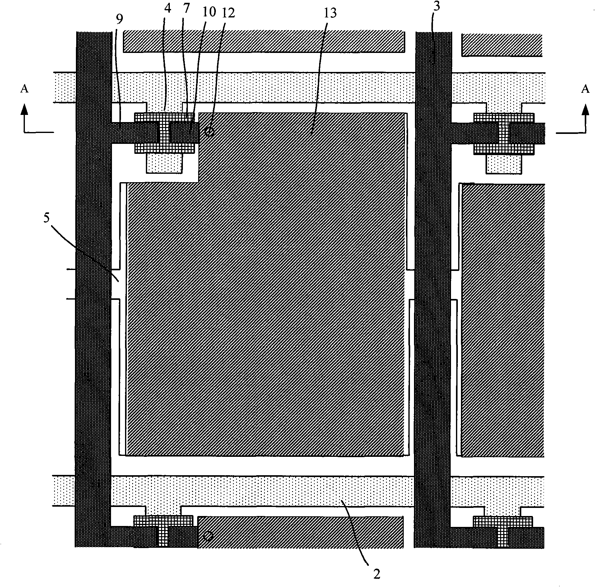
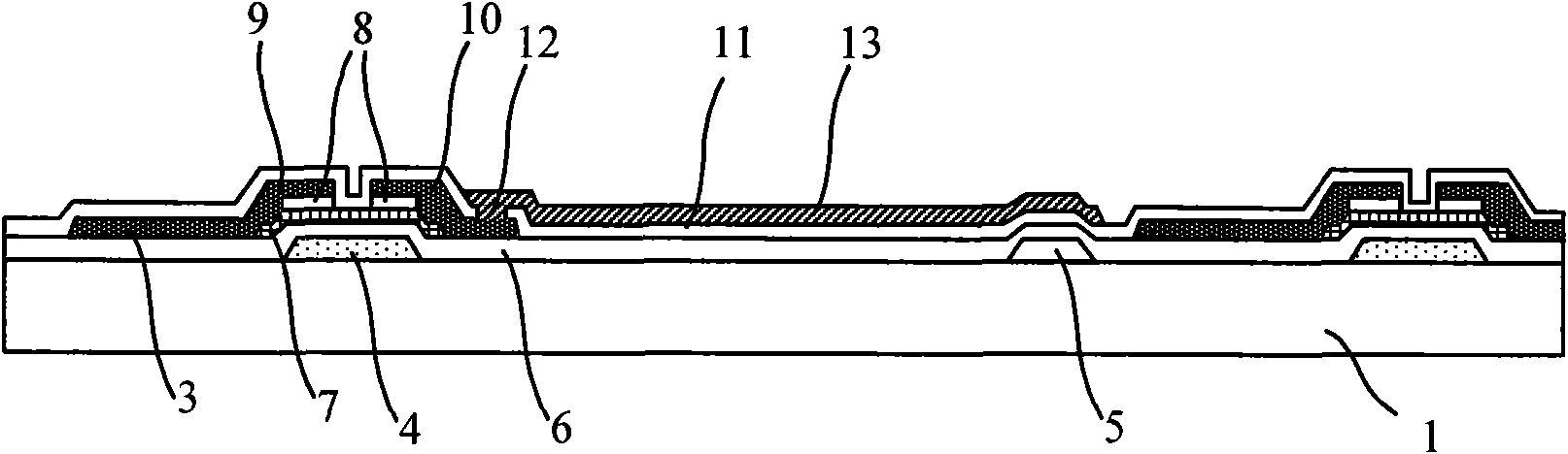
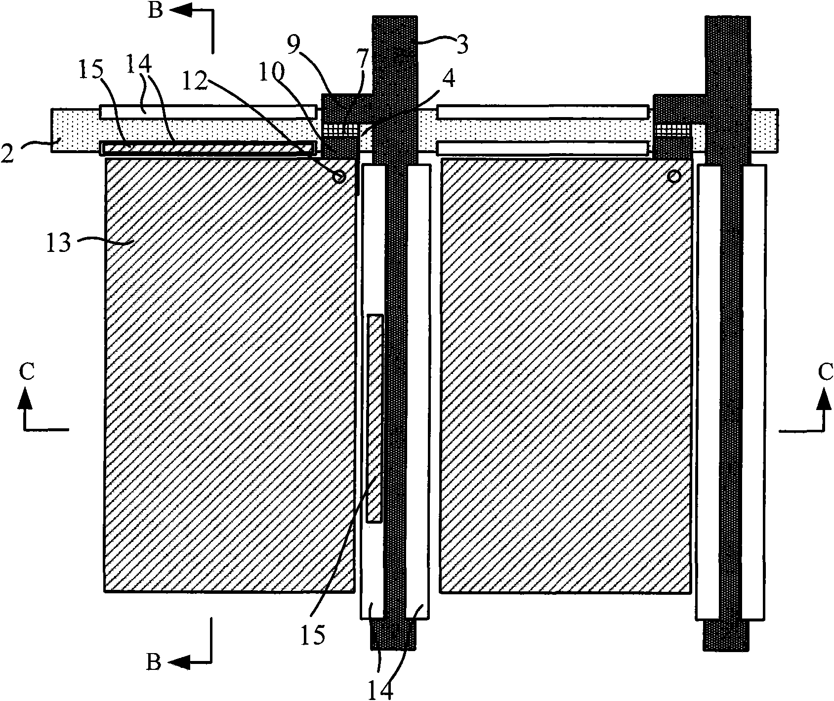
[0043] image 3 is a partial top view structure schematic diagram of the first embodiment of the array substrate of the present invention, Figure 4 for image 3 The B-B direction sectional view in Figure 5 for image 3 C-C in the sectional view. The array substrate of this embodiment is specifically the array substrate in TFT-LCD, and its main structure includes: base substrate 1 and the multi-thin film layer on it, the passivation layer 11 is covered on the multi-thin film layer, on the passivation layer 11 A plurality of pixel electrodes 13 in a matrix form are formed corresponding to each pixel region. The base substrate 1 is generally a glass substrate. The multi-thin film layer is a structure used to control the voltage on each pixel electrode 13 so as to prese...


PUM


Abstract

The invention relates to an array substrate as well as a manufacturing method and a liquid crystal display panel thereof. A groove is formed on a passivation layer of the array substrate and correspondingly formed between two adjacent pixel electrodes; and the depth of the groove is less than that of the passivation layer. The method comprises the following steps of: forming patterns with a plurality of film layers on the substrate; forming the passivation layer on the substrate with the plurality of film layers forming; forming a passivation layer through hole and the groove on the passivation layer; depositing a transparent conducting film layer on the passivation layer with the groove forming; and forming a plurality of pixel electrodes in a matrix mode by adopting a mapping process. The liquid crystal display panel comprises the array substrate. In the invention, the groove is formed on the passivation layer beyond the pixel electrode area, therefore, a pixel electrode material layer can form a faultage at the edge of the groove, and the connected short-circuit between the adjacent pixel electrodes is reduced or avoided, thereby improving the finished product ratio.

Description

technical field [0001] The invention relates to liquid crystal display technology, in particular to an array substrate, a manufacturing method thereof, and a liquid crystal panel. Background technique [0002] Liquid crystal displays play an important role in flat panel displays, and a thin film transistor liquid crystal display (Thin Film Transistor-Liquid Crystal Display; hereinafter referred to as TFT-LCD) is a widely used liquid crystal display. [0003] The liquid crystal panel of TFT-LCD is composed of an array substrate and a color film substrate. figure 1 It is a partial top view structure schematic diagram of a thin film transistor liquid crystal display array substrate in the prior art, figure 2 for figure 1 A-A in the sectional view. Such as figure 1 with figure 2 As shown, a typical TFT-LCD array substrate structure mainly includes: a base substrate 1; the pattern of the gate electrode 4 and the gate scanning line 2 is formed on the base substrate 1, and t...

Claims


Application Information

Patent Timeline
IPC IPC(8): G02F1/1362H01L23/528H01L21/768H01L21/84
Inventor 谢振宇林承武陈旭刘翔
Owner BEIJING BOE OPTOELECTRONCIS TECH CO LTD
Why Eureka
Try Eureka