Semiconductor device and method of manufacturing the same

a semiconductor and semiconductor technology, applied in the field of semiconductor devices, can solve the problems of inability to accurately display images, inability to uniformly irradiate regions of semiconductors with laser light, and inability so as to reduce the influence of crystal state fluctuation, the effect of reducing the fluctuation of laser light irradiation number

Inactive Publication Date: 2005-08-16
SEMICON ENERGY LAB CO LTD
View PDF14 Cites 20 Cited by
  • Summary
  • Abstract
  • Description
  • Claims
  • Application Information

AI Technical Summary

Benefits of technology

[0023]The present invention has been made in view of the above, and an object of the present invention is therefore to provide a semiconductor device free of the above problems and a method of manufacturing the semiconductor device. Specifically, an object of the present invention is to provide a semiconductor device and a method of manufacturing the same which can reduce influence of fluctuation in characteristic among transistors due to fluctuation in laser light irradiation number and laser light intensity on a semiconductor. Another object of the present invention is to provide a semiconductor device with less laser fringes and a method of manufacturing the semiconductor device.
[0055]In the present invention, semiconductors are placed in parallel to Direction x (the laser light scanning direction) to even out fluctuation in characteristic between a transistor in one point in Direction x (the laser light scanning direction) and a transistor in another point. By arranging transistors in parallel to Direction x (the laser light scanning direction), channel formation regions of the transistors are irradiated with a laser in an increased number of times. This reduces fluctuation in laser light irradiation number and accordingly reduces fluctuation in crystal state between the semiconductors. Influence of fluctuation in characteristic among the transistors having the above semiconductors thus can be lowered.
[0056]Furthermore, in the present invention, each semiconductor is arranged so as to stretch over at least two pixels in order to increase the number of times the semiconductor is irradiated with the laser. This makes the length of the semiconductor larger than the pixel pitch of the pixels. By thus increasing the transistor size and, for example, setting a channel length L larger than the channel width, fluctuation in transistor itself can be reduced.
[0057]The width and length of laser light and the laser scan pitch in irradiating the semiconductors are not particularly limited. However, since the semiconductors are irradiated with a laser an increased number of times in the present invention, widening the laser light and measures to the similar effect are preferable. This makes it possible to further reduce fluctuation in crystal state between the semiconductors. If each semiconductor is sufficiently long, the laser light irradiation number for each semiconductor can be satisfactorily large and fluctuation among transistors is reduced even when the laser scan pitch is somewhat larger. In this way, a semiconductor device is manufactured without increasing the total number of laser light irradiation for irradiating the entire pixel portion. As a result, processing speed in manufacture of a semiconductor device is raised and therefore the cost is lowered.

Problems solved by technology

This means that regions of a semiconductor cannot be irradiated uniformly with laser light even if they receive the same number of laser light irradiation.
Such light emitting display is incapable of displaying an image in accurate gray scales.

Method used


Image

  • Semiconductor device and method of manufacturing the same
  • Semiconductor device and method of manufacturing the same
  • Semiconductor device and method of manufacturing the same

Examples


embodiment mode 1

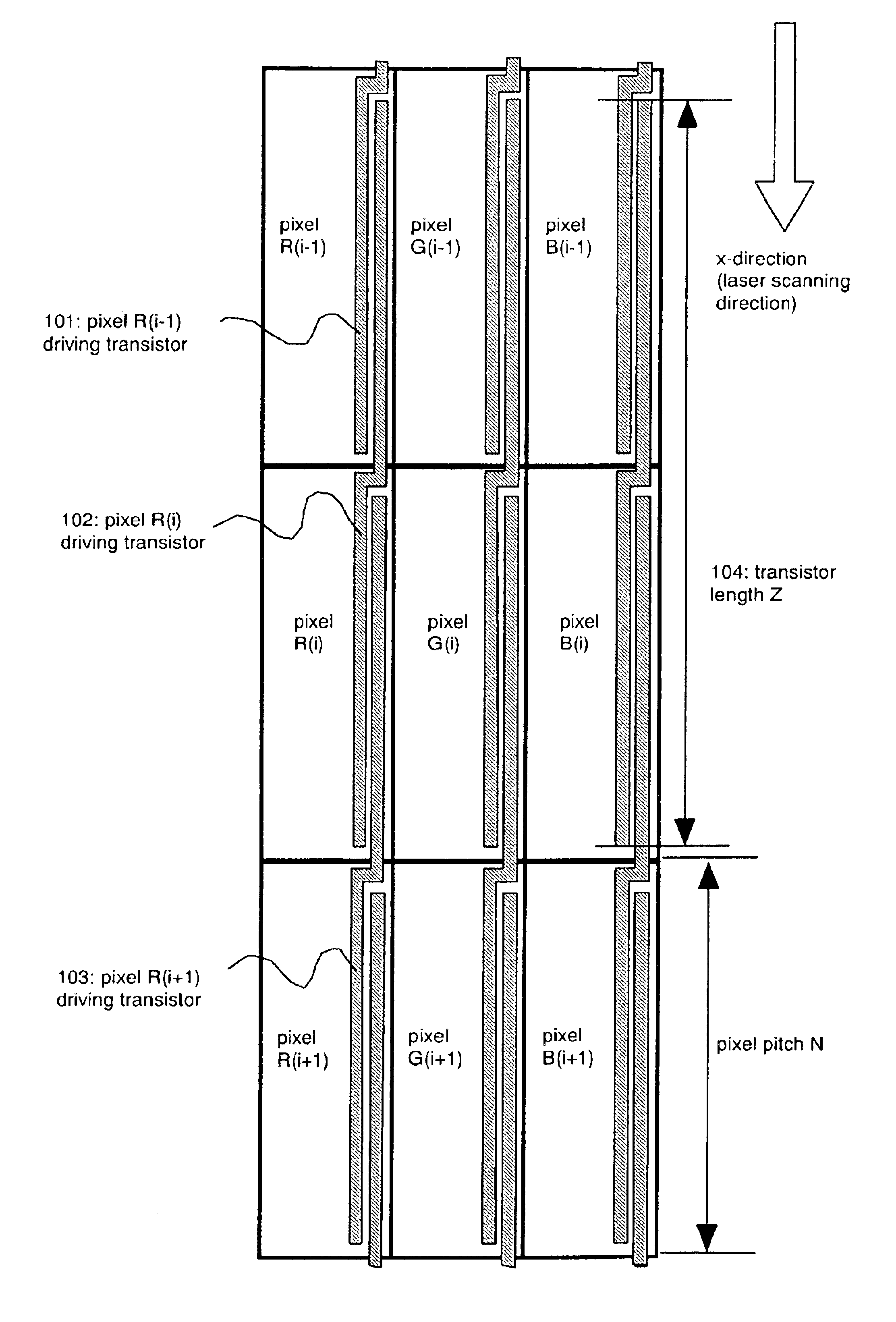
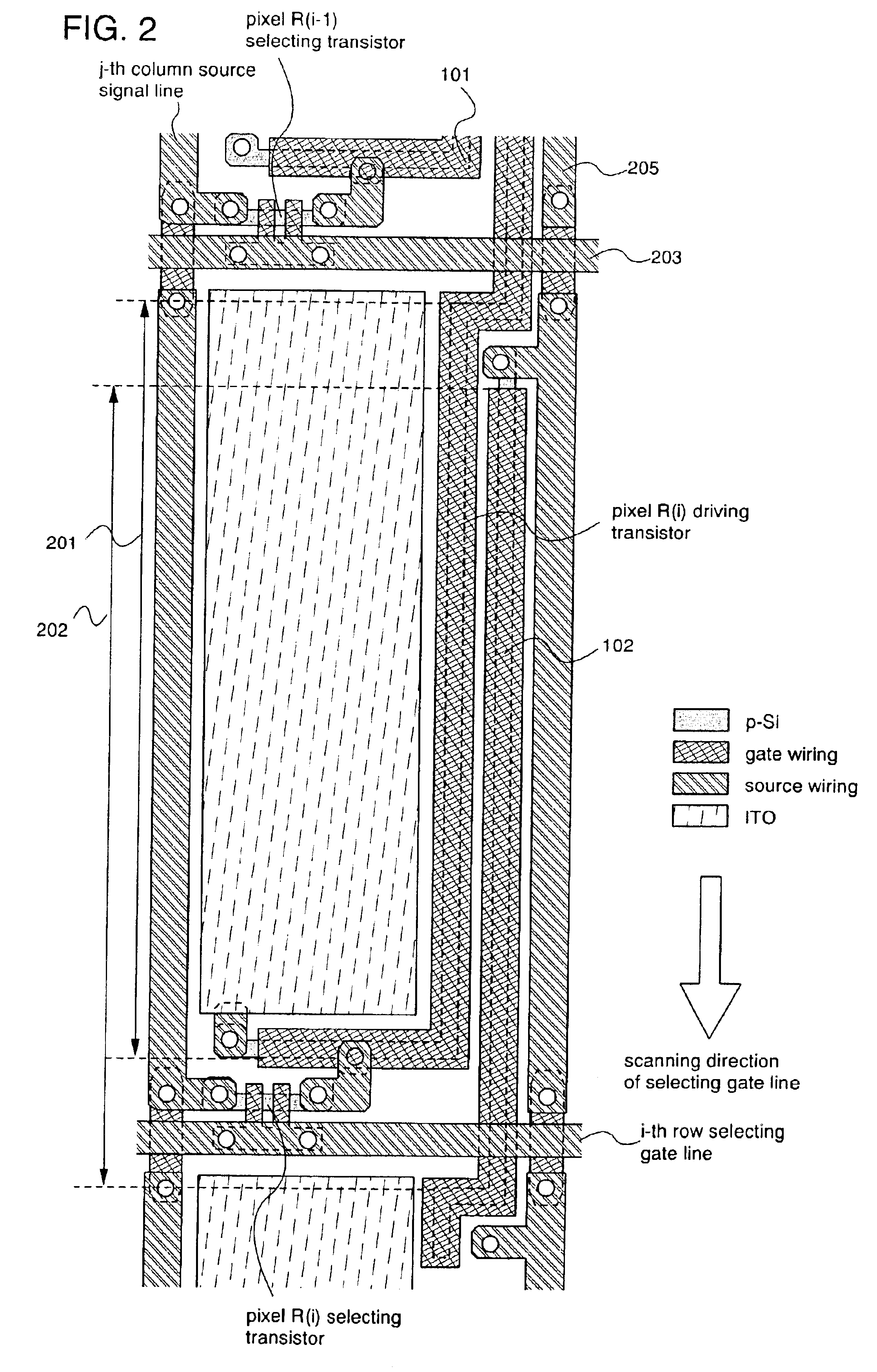
[0094]An embodiment mode of a semiconductor device according to the present invention will be described with reference to FIGS. 1 to 6. FIG. 1 is a schematic diagram of arrangement of transistors in pixels. FIG. 1 shows three pixels for red, green, and blue arranged in accordance with the stripe arrangement. However, the number of pixels in FIG. 1 will be nine if one pixel is to have one color. For discrimination, the R color portion of the first pixel from the top of FIG. 1 is referred to as pixel R(i−1), the G color portion thereof is pixel G(i−1), and the B color portion thereof is pixel B(i−1). Similarly, the R color portion of the second pixel from the top is referred to as pixel R(i), the G color portion thereof is G(i), and the B color portion thereof is pixel B(i). The R color portion of the third pixel from the top is referred to as pixel R(i+1), the G color portion thereof is G(i+1), and the B color portion thereof is pixel B(i+1).

[0095]Each pixel has transistors. For inst...

embodiment mode 2

[0120]This embodiment gives a description with reference to FIGS. 7 to 11 on arrangement of driving transistors which is different from that of Embodiment Mode 1. FIG. 7 is a schematic diagram of arrangement of transistors in pixels.

[0121]In FIG. 7, a driving transistor of each pixel is placed so as to reach a region of a surrounding pixel and two transistors are connected in series or parallel to work as one transistor. Therefore a pixel R(i+1) driving transistor 2704 and a pixel R(i) driving transistor 1701 are placed in a pixel R(i). A pixel R(i) driving transistor 2702 is placed in a pixel R(i−1). The pixel R(i) driving transistor 1701 and the pixel R(i) driving transistor 2702 are electrically connected to each other. In this manner, a driving transistor of one pixel is placed in the one pixel and a pixel above in FIG. 7 and the driving transistor in the one pixel and the driving transistor in the above pixel are electrically connected to each other.

[0122]The length of a drivin...

embodiment mode 3

[0141]The above embodiment modes describe novel arrangement for transistors. In this embodiment mode, novel arrangement for selecting gate lines will be described with reference to FIGS. 12 to 15B. FIG. 12 is a schematic diagram of arrangement of transistors in pixels. FIG. 12 shows two pixels arranged in accordance with the stripe arrangement. However, the number of pixels in FIG. 12 will be six if one pixel is to have one color. For discrimination, the R color portion of the first pixel from the top of FIG. 12 is referred to as pixel R1, the G color portion thereof is pixel G1, and the B color portion thereof is pixel B1. Similarly, the R color portion of the second pixel from the top is referred to as pixel R2, the G color portion thereof is G2, and the B color portion thereof is pixel B2.

[0142]Each pixel has transistors. For instance, the pixel G1 has a transistor for driving a light emitting element of the pixel. This transistor is called a pixel G1 driving transistor 1201. Sim...


PUM


Abstract

To obtain a semiconductor device and a method of manufacturing the same which can reduce influence of fluctuation in characteristic among transistors due to fluctuation in laser light irradiation number and laser light intensity on a semiconductor. There is provided a semiconductor device with plural pixels having transistors forming a matrix pattern, in which: the transistors have semiconductors crystallized by laser light irradiation; the semiconductors stretch over at least two pixels; the length of each of the semiconductors is longer than the pixel pitch of the pixels; and when the scan pitch of the laser light is given as M and the pixel pitch of the pixels is given as N, the semiconductors are irradiated with the laser light N / M times or more.

Description

BACKGROUND OF THE INVENTION[0001]1. Field of the Invention[0002]The present invention relates to a semiconductor device and a method of manufacturing the same. Specifically, the present invention relates to a semiconductor device in which a transistor is formed from a polycrystalline semiconductor crystallized by laser light irradiation and to a method of manufacturing the semiconductor device. The invention also relates to a semiconductor device which uses the above transistor in its pixel and to a method of manufacturing the semiconductor device.[0003]2. Description of the Related Art[0004]In recent years, portable equipment such as PDAs, cellular phones, and notebook computers have grown popular. Such equipment has flat panel displays mounted thereto. Flat panel displays employed often are STN liquid crystal displays, amorphous silicon TFT (amorphous silicon thin film transistor) liquid crystal displays, and the like. However, lately these displays have been taken over by low tem...

Claims


Application Information

Patent Timeline
Patent Type & Authority Patents(United States)
IPC IPC(8): H01L21/70H01L27/12H01L21/84H01L27/32H01L27/15H01L27/28H01L21/77
CPCH01L27/12H01L27/1285H01L27/156H01L27/3211H01L27/3244H10K59/35H10K59/12
Inventor KIMURA, HAJIMEANZAI, AYAYAMAZAKI, SHUNPEI
Owner SEMICON ENERGY LAB CO LTD
Why Eureka
Try Eureka