Manufacturing method of SiC-based super-junction IGBT (Insulated Gate Bipolar Transistor) with low off-state loss

A fabrication method and off-state technology, applied in semiconductor/solid-state device manufacturing, semiconductor devices, electrical components, etc., can solve problems such as charge-imbalanced Si-based superjunction devices, reduce ion implantation processes, improve on-state characteristics and good performance. efficiency, and the effect of optimizing the cell structure of the device

Inactive Publication Date: 2016-10-12
GLOBAL POWER TECH CO LTD
View PDF5 Cites 2 Cited by
  • Summary
  • Abstract
  • Description
  • Claims
  • Application Information

AI Technical Summary

Problems solved by technology

[0003] Although power devices such as Si-based superjunction MOSFETs have been developed for several years, the charge imbalance problem they face limits the application of Si-based superjunction devices in higher voltage fields.

Method used


Image

  • Manufacturing method of SiC-based super-junction IGBT (Insulated Gate Bipolar Transistor) with low off-state loss
  • Manufacturing method of SiC-based super-junction IGBT (Insulated Gate Bipolar Transistor) with low off-state loss
  • Manufacturing method of SiC-based super-junction IGBT (Insulated Gate Bipolar Transistor) with low off-state loss

Examples


no. 1 example

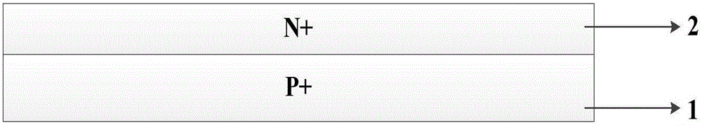
[0030] Before making the SiC-base superjunction IGBT with low off-state loss of the present invention, earlier RCA cleans the p+ type substrate 1 of SiC (referring to figure 2 ). Specifically:

[0031] (a) Ultrasonic cleaning with acetone and ethanol in sequence, followed by rinsing with deionized water.

[0032] (b) Boiling the SiC substrate 1 after organic ultrasonication in concentrated sulfuric acid and hydrogen peroxide solution for at least 10 minutes.

[0033] (c) Boil the substrate 1 boiled in concentrated sulfuric acid with No. 1 solution and No. 2 solution for more than 10 minutes respectively, rinse it with deionized water, and dry it with nitrogen gas for use. The No. 1 liquid is a mixture of ammonia, hydrogen peroxide and deionized water, and the No. 2 liquid is a mixture of hydrochloric acid, hydrogen peroxide and deionized water.

[0034] (d) Soak the rinsed substrate in hydrofluoric acid for at least 1 min to remove the surface oxide layer.

[0035] The do...

no. 2 example

[0070] The cleaning of the SiC p+ type substrate 1 before fabricating the SiC-based super-junction IGBT with low off-state loss of the present invention is the same as that of the first embodiment, and will not be repeated here.

[0071] The doping concentration of the p+ type substrate 1 needs to meet a specific value to meet a certain injection efficiency, which is roughly 1×10 18 cm -3 ~3×10 18 cm -3 , SiC p+-type substrate 1 can undergo a series of thinning, grinding, polishing, cleaning and other processes on the sample through mechanical processing and chemical reaction methods, so that the surface of the sample can reach the required thickness and flatness.

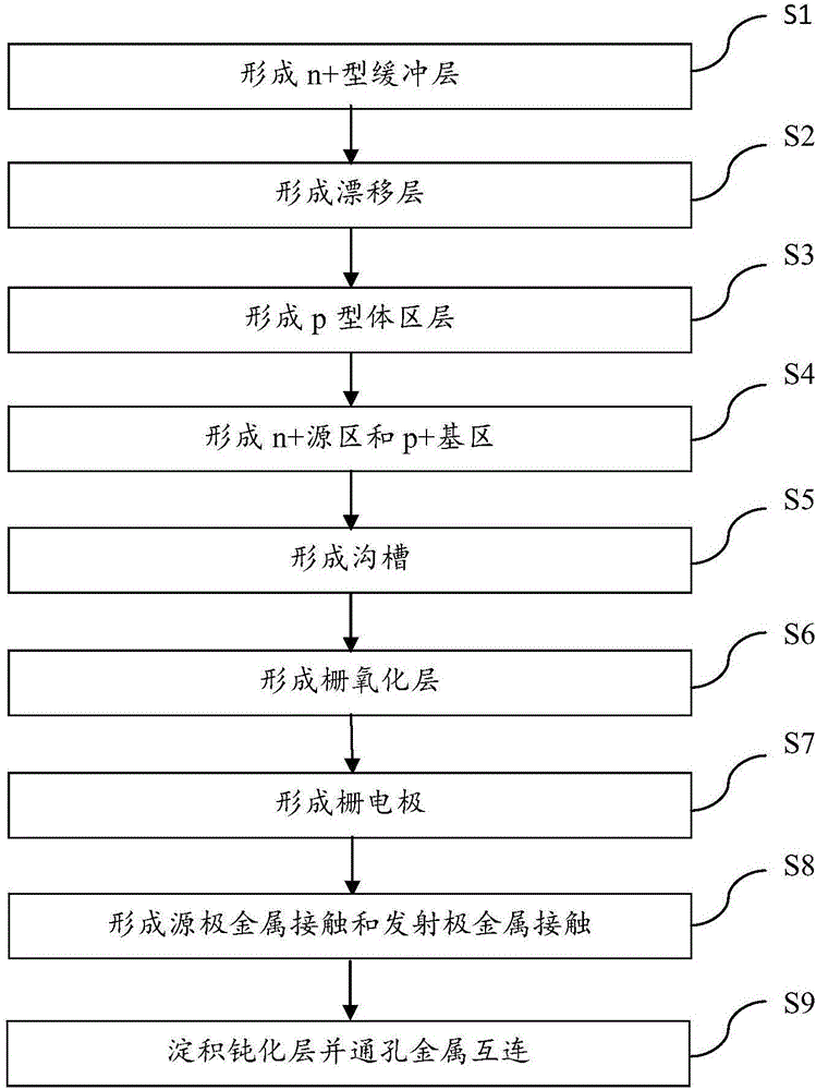
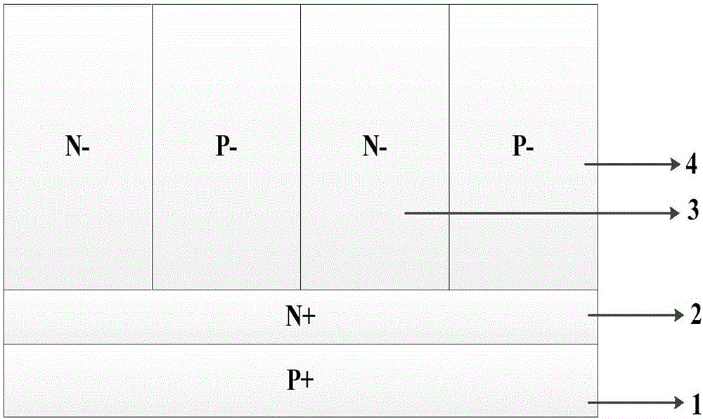
[0072] S1: Refer to figure 2 , epitaxially grow n+ type buffer layer 2 on SiC p+ type substrate 1 by chemical vapor deposition or other methods of epitaxially growing materials. The source of epitaxial growth is silane or trichlorosilane, ethylene, etc. or propane, etc., the thickness of the n+ type buffer lay...

no. 3 example

[0077] The cleaning of the SiC p+ type substrate 1 before fabricating the SiC-based super-junction IGBT with low off-state loss of the present invention is the same as that of the first embodiment, and will not be repeated here.

[0078] The doping concentration of the p+ type substrate 1 needs to meet a specific value to meet a certain injection efficiency, which is roughly 6.5×10 17 cm -3 ~8.5×10 17 cm -3 , SiC p+-type substrate 1 can undergo a series of thinning, grinding, polishing, cleaning and other processes on the sample through mechanical processing and chemical reaction methods, so that the surface of the sample can reach the required thickness and flatness.

[0079] S1: Refer to figure 2 , epitaxially grow n+ type buffer layer 2 on SiC p+ type substrate 1 by chemical vapor deposition or other methods of epitaxially growing materials. The source of epitaxial growth is silane or trichlorosilane, ethylene, etc. or propane, etc., the thickness of the n+ type buffer...


PUM

PropertyMeasurementUnit
thicknessaaaaaaaaaa
thicknessaaaaaaaaaa
thicknessaaaaaaaaaa

Abstract

The invention relates to a manufacturing method of a SiC-based super-junction IGBT (Insulated Gate Bipolar Transistor) with low off-state loss. The manufactured SiC-based super-junction IGBT has low off-state loss. The manufacturing method comprises the steps of epitaxially growing a buffer layer of a first conductivity type at a SiC substrate of a second conductivity type; forming a drifting layer containing column regions of the first conductivity type and columns regions of the second conductivity type on the buffer layer, wherein the columns regions of the first conductivity type and the column regions of the second conductivity type are alternatively arranged in the transverse direction; epitaxially forming a body region layer of the second conductivity type on the drifting layer; forming a source region of the first conductivity type on the body region layer through ion implantation or epitaxial growth, and forming a base region of the second conductivity type through ion implantation; etching the SiC substrate so as to form a trench, wherein the trench crosses the body region layer and gets into the column region in depth; forming a gate oxidation layer in the trench; forming a gate electrode in the trench; forming source electrode metal contact in the source region and the base region, forming transmitting electrode metal contact in reverse side of the SiC substrate, and forming ohmic contact; and depositing a passivation layer on the grate electrode and the source electrode metal contact, and through-hole metal interconnection is performed.

Description

technical field [0001] The invention relates to a method for manufacturing a SiC-based high-power device, in particular to a method for manufacturing a SiC-based super-junction insulated gate bipolar transistor (SJIGBT) device with lower off-state loss. Background technique [0002] The third-generation semiconductor silicon carbide (SiC) has superior physical and electrical properties compared to traditional Si, such as wide band gap, high breakdown field strength, and high thermal conductivity. Therefore, SiC-based high-power devices can alleviate the problems of high dynamic loss and static loss faced by Si power devices, and occupy a core position in the field of high-power, high-frequency, and high-temperature power electronics. [0003] Although power devices such as Si-based superjunction MOSFETs have been developed for several years, the charge imbalance problem they face limits the application of Si-based superjunction devices in higher voltage fields. In recent ye...

Claims


Application Information

Patent Timeline
Patent Type & Authority Applications(China)
IPC IPC(8): H01L21/331H01L21/266
CPCH01L29/66325H01L21/266
Inventor 申占伟张峰陈彤
Owner GLOBAL POWER TECH CO LTD
Why Eureka
Try Eureka