Wideband dual amplifier circuits

a dual-amplifier and amplifier technology, applied in the direction of amplifiers, amplifiers with semiconductor devices only, amplifiers with semiconductor devices, etc., can solve the problems of phase discontinuities, limited mtj's ability to amplify low-level current input signals over a wide range of frequencies, and low gain respons

Inactive Publication Date: 2002-03-12
IBM CORP
View PDF13 Cites 13 Cited by
  • Summary
  • Abstract
  • Description
  • Claims
  • Application Information

AI Technical Summary

Benefits of technology

A FET and MTJ are connected in functional cascade to best utilize the amplification, impedance, noise, and operating mode characteristics of each device. This composite utilizes a synergistic improvement in the gain bandwidth of such cascaded pair. In one form the MTJ input is the load of the FET. In another form, the FET input (gate electrode) is the load of the MTJ. The FET / MTJ composite matches respective desirable impedance characteristics while eliminating the noise introduced by resistors in conventional cascade configurations.

Problems solved by technology

Additionally, a gain-bandwidth product as well as a noise factor of a magnetic tunnel junction device (hereinafter "MTJ") limits the MTJ's ability to amplify low-level current input signals over a wide range of frequencies.
However, that gain responses are not flat and often have phase discontinuities.
Furthermore, the noise performance is poorer when stages are cascaded.

Method used


Image

  • Wideband dual amplifier circuits
  • Wideband dual amplifier circuits
  • Wideband dual amplifier circuits

Examples


Embodiment Construction

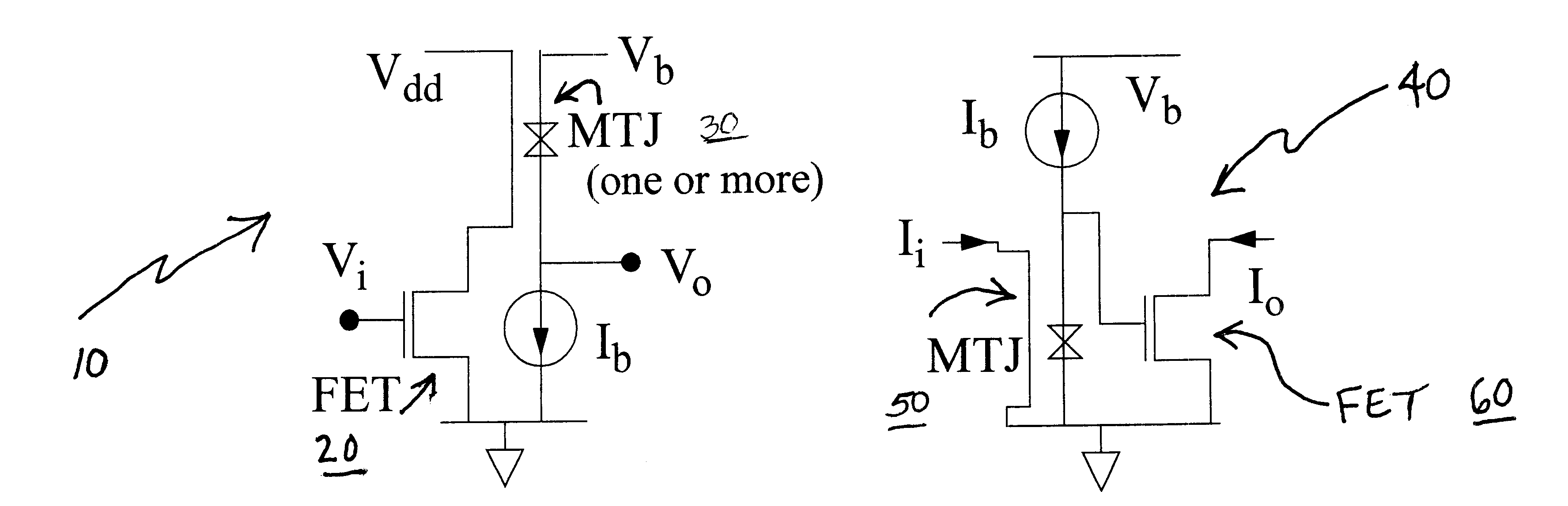
Two electrical circuits are said to be dual of one another if they obey identical circuit equations, but with the roles of current and voltages interchanged. In general, a dual circuit can be constructed by the parameter / configuration interchanges set forth in TABLE 1.

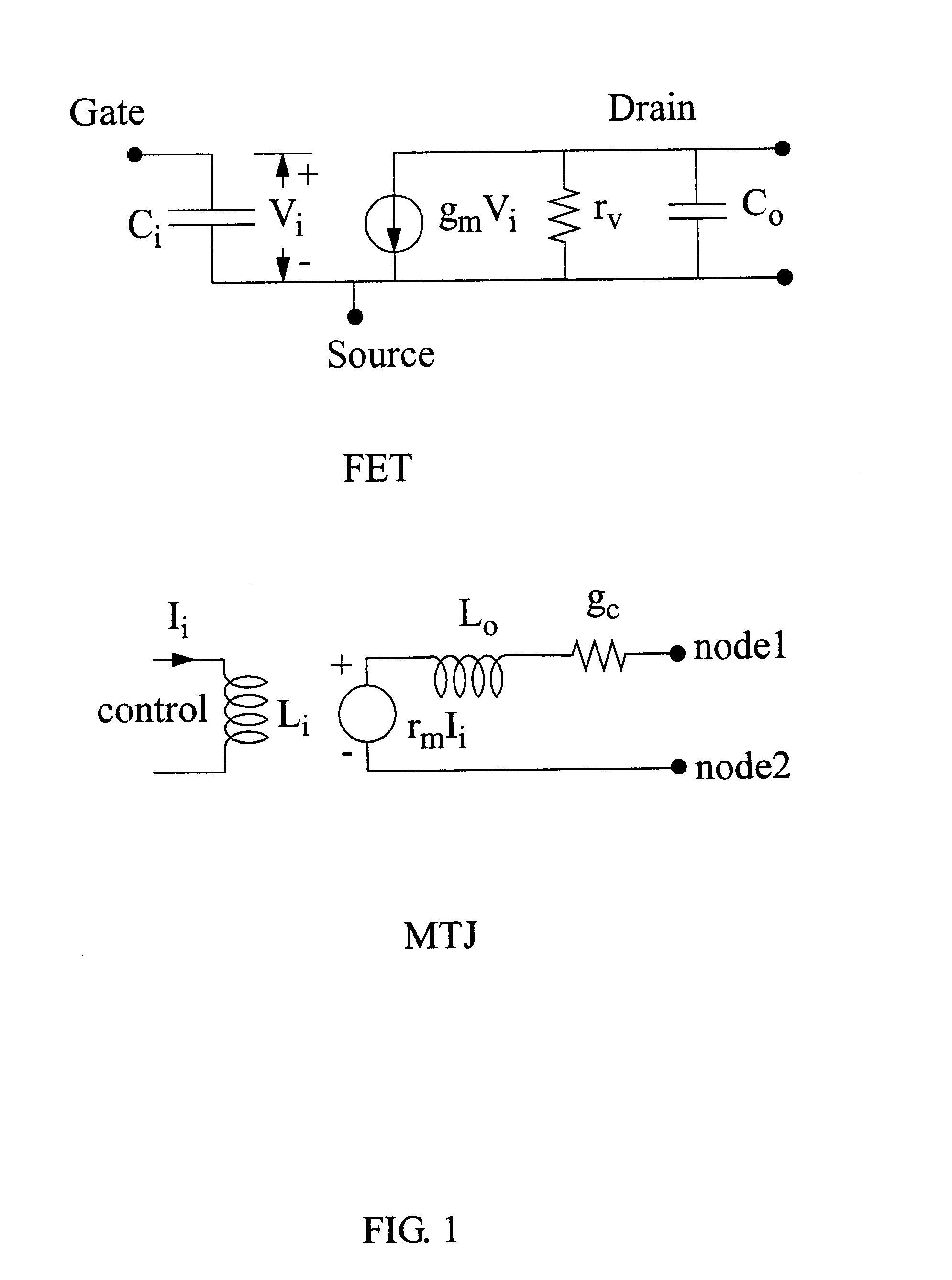
The semiconductor field-effect transistors and the magnetic tunnel junction behave like active dual elements. The FETs are voltage-controlled, i.e. the voltage at the gates control the channel (output) currents, the gate poses a capacitive impedance, and the differential channel impedance is high--ideally a current source. The MTJs are current-controlled, i.e. current through the control lines controls the output voltages, the control lines poses an inductive impedance, and the differential channel impedance is low--ideally a voltage source.

The important small-signal parameters for the FET and MTJ are listed in TABLE 2.

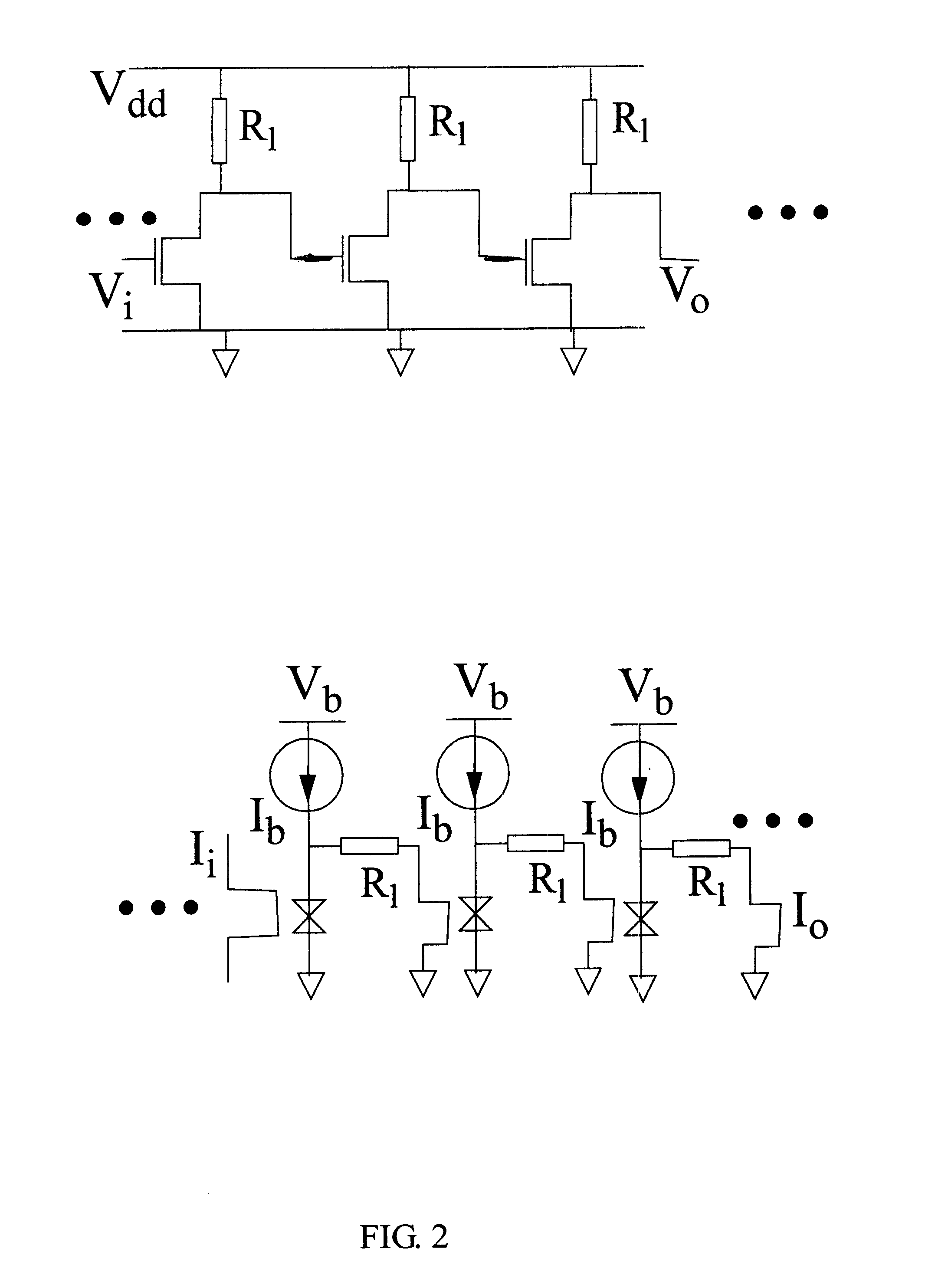
If one were to cascade individual FET amplifier stages or the MTJ stages as depicted in FIG. 2, one w...


PUM


Abstract

Dual amplifying circuits having a magnetic tunnel junction device and a field effect transistor configured in a complementing set are disclosed herein. In one embodiment, the field effect transistor is operable to control a current level of a current operating signal flowing through the magnetic tunnel junction device. In another embodiment, the magnetic tunnel junction device is operable to control a voltage level of a voltage signal being applied to a gate terminal of the field effect transistor. The gain-bandwidth product of both embodiments is greater than the individual gain-bandwidth products of the individual devices through the elimination of noise contributing resistive type circuit elements.

Description

1. Field of the InventionThe present invention generally relates to amplifier circuits providing wideband amplification with minimal noise, and in particular, to amplifier circuits utilizing pairs of functionally complementing devices.2. Description of the Related ArtA gain-bandwidth product as well as a noise factor of a field effect transistor (hereinafter "FET") limits the FET's ability to amplify low-level voltage input signals over a wide range of frequencies. Additionally, a gain-bandwidth product as well as a noise factor of a magnetic tunnel junction device (hereinafter "MTJ") limits the MTJ's ability to amplify low-level current input signals over a wide range of frequencies.In radio frequency and microwave circuits, the gain of amplifiers utilizing a FET or MTJ as an active filter can be increased by narrowing the pass band of the FET or MTJ. However, that gain responses are not flat and often have phase discontinuities. Furthermore, the noise performance is poorer when st...

Claims


Application Information

Patent Timeline
Patent Type & Authority Patents(United States)
IPC IPC(8): H03F19/00H03F3/193
CPCH03F19/00H03F9/02
Inventor GHOSHAL, UTTAM S.
Owner IBM CORP
Why Eureka
Try Eureka