Method and apparatus for transferring semiconductor substrates using an input module

Inactive Publication Date: 2002-03-26
APPLIED MATERIALS INC
View PDF11 Cites 62 Cited by
  • Summary
  • Abstract
  • Description
  • Claims
  • Application Information

AI Technical Summary

Benefits of technology

To facilitate understanding, identical reference numerals have been used, wh

Problems solved by technology

The traditional, horizontal paddle and retention mechanisms, while functional for passing substrates among certain semiconductor processing stages, are cumbersome when directed for use between certain types of semiconductor processing stages.
If the slurry dries and hardens on the substrate surface, the substrate may become damaged, defective or unfit for further processing.
The 90 degrees difference in substrate orientation between the polishing and cleaning processes le

Method used


Image

  • Method and apparatus for transferring semiconductor substrates using an input module
  • Method and apparatus for transferring semiconductor substrates using an input module
  • Method and apparatus for transferring semiconductor substrates using an input module

Examples


Embodiment Construction

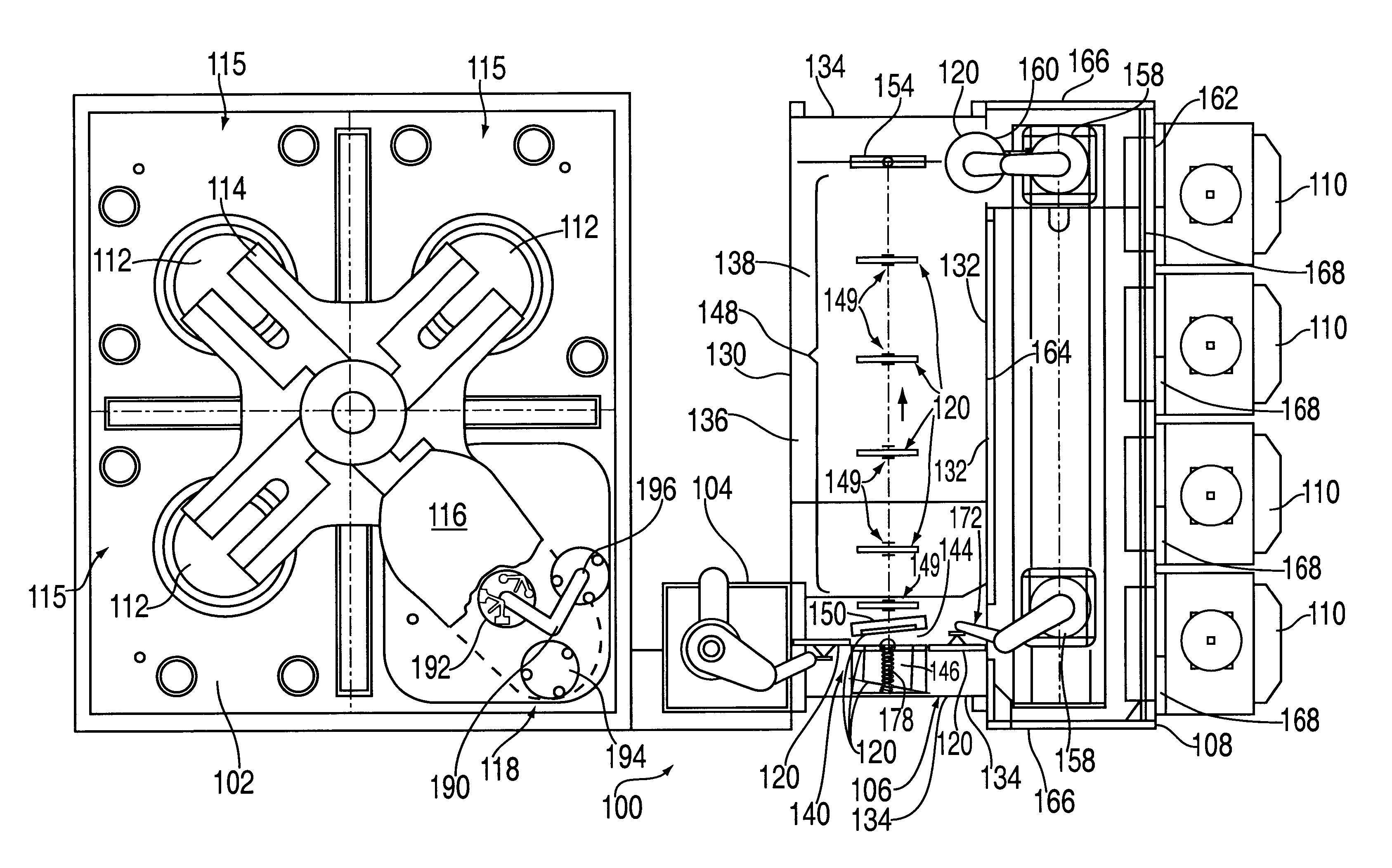
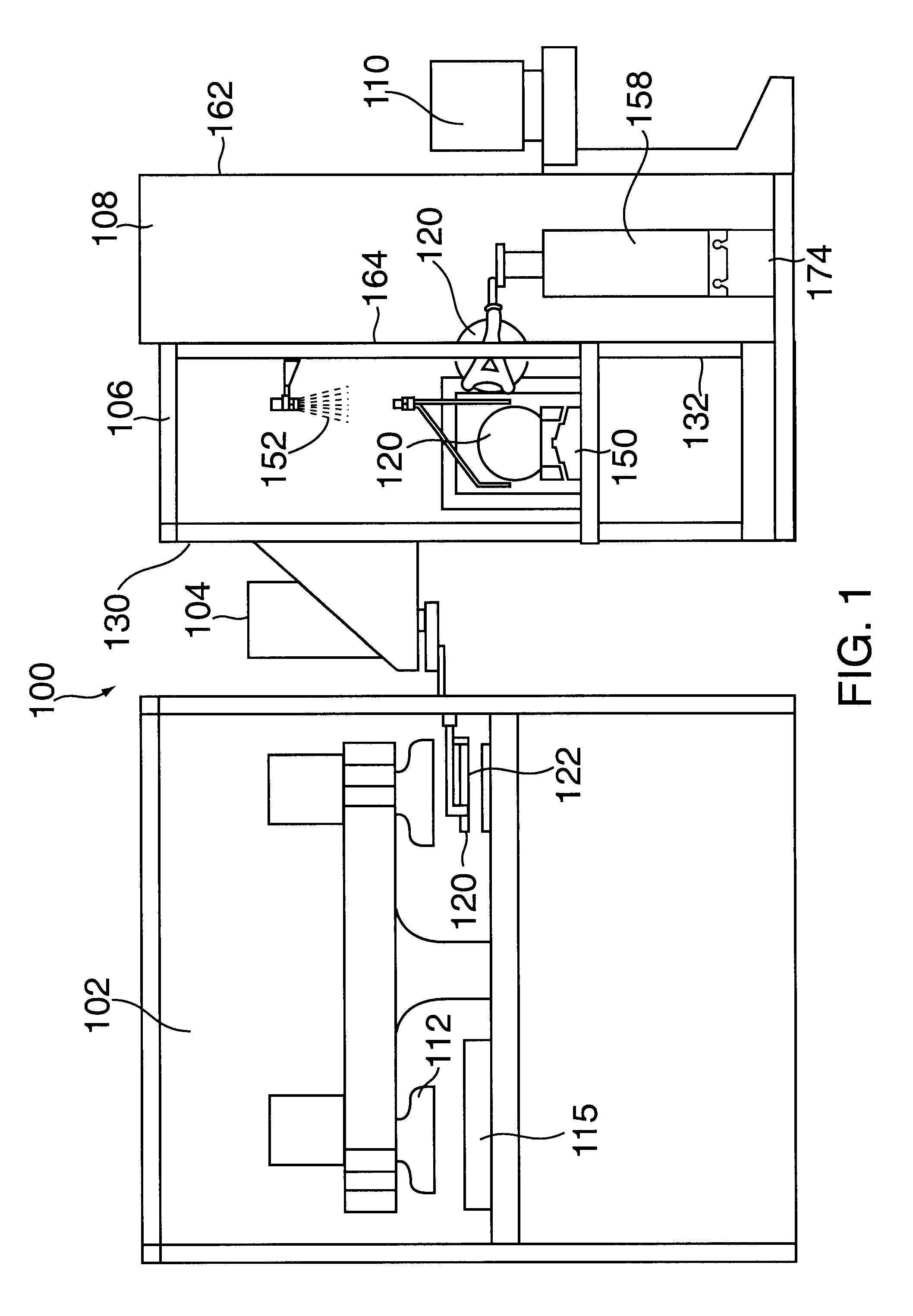
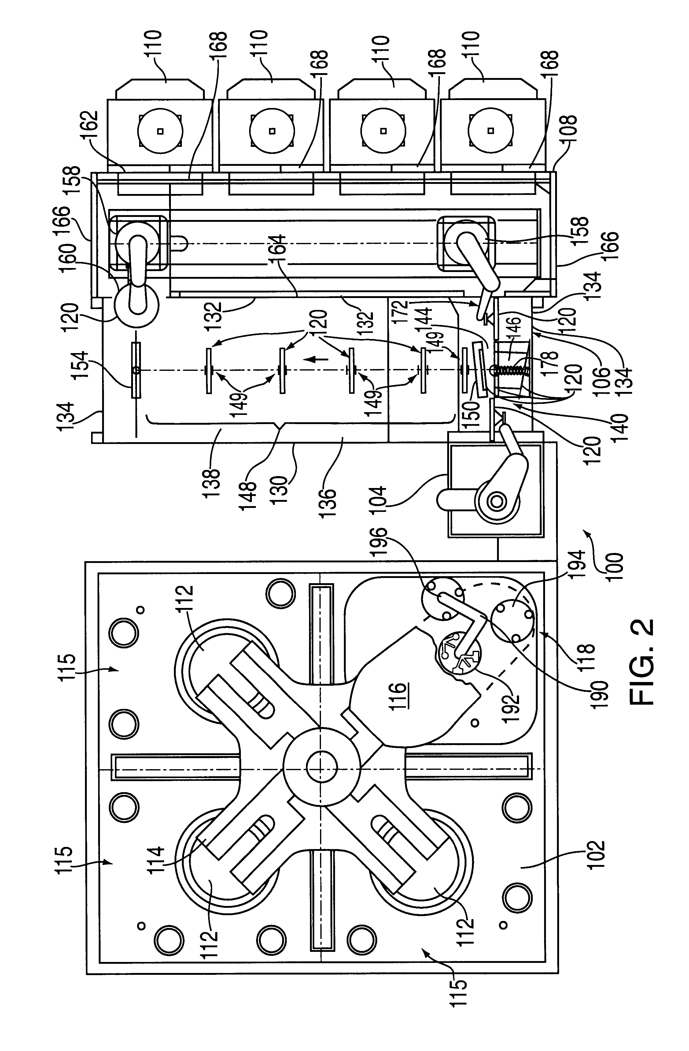
FIGS. 1 and 2 depict an exemplary semiconductor wafer chemical mechanical polishing system (CMP system) 100. The reader is encouraged to simultaneously refer to both FIGS. 1 and 2 to achieve the greatest understanding of the invention. The CMP system 100 is generally comprised of modules, including, for example, one or more polishing modules 102, a first or wet robot 104, a cleaning module 106, a factory interface module 108, and one or more wafer storage cassettes 110 (four cassette 110 are shown). Alternatively, other polishing systems having varied configurations may be devised by one skilled in the art that include fewer or additional modules.

The factory interface module 108 is generally substantially rectangular in shape having a first wall 162, a second wall 164 and lateral walls 166. The first wall 162 includes a plurality of bays 168 adapted to interface with at least one of the wafer cassettes 110. The second wall 164 mates against a back wall 132 of the cleaning module 106...


PUM


Abstract

A semiconductor substrate processing method and apparatus, more specifically, a method and apparatus for polishing a substrate or semiconductor wafer in a polishing system. In one embodiment, the system includes one or more polishing modules, an input module, a first robot and a second robot that provides a compact polishing system that has a minimal tool footprint. The first robot is adapted to transfer the substrate to the input module, while the second robot is adapted to transfer the substrate between the input module and the one or more polishing modules. In another embodiment, the first and second robots have rotary actuators coupled to their grippers that enable the substrate to be orientated between a horizontal and vertical position. The input module is adapted to maintain the substrate in a vertical orientation. The vertical orientation of the substrates facilitates integration of a cleaning system that cleans the substrates while in the vertical orientation.

Description

BACKGROUND OF THE DISCLOSURE1. Field of InventionThe present invention relates generally to a semiconductor substrate processing system. More specifically, the invention relates to a method and apparatus for polishing a semiconductor substrate.2. Description of the Background ArtIn semiconductor substrate processing, the transfer of substrates between modules is required to optimize processing rates while minimizing risk of substrate damage and contamination. The typical method of transferring a substrate between processing and support equipment is to move the substrate using a paddle manipulated by a robot. In most instances, the substrate is lifted from a pedestal using pins to allow the paddle to be positioned under the center portion of the substrate. In other modules, such as transfer cassettes, the substrate is supported horizontally at the edges, allowing the paddle access under the substrate. The paddle is then lifted to engage the substrate and carry the substrate from one ...

Claims


Application Information

Patent Timeline
IPC IPC(8): B24B37/04H01L21/67H01L21/673H01L21/687H01L21/677B24B37/34H01L21/304
CPCB24B37/345H01L21/68707H01L21/67313H01L21/67219
Inventor ETTINGER, GARYWIESE, GREGSHANMUGASUNDRUM, ARULKUMAR
Owner APPLIED MATERIALS INC
Why Eureka
Try Eureka