Self aligned dual damascene method

a dual damascene and self-aligning technology, applied in the field of dual damascene methods, can solve the problems of limited further development, difficulty in patterning the second photoresist, and disadvantages of conventional self-aligning dual damascene methods, and achieve the effects of decreasing etching aspect ratio, increasing process windows, and small line width

Inactive Publication Date: 2002-04-02
TAIWAN SEMICON MFG CO LTD +1
View PDF10 Cites 49 Cited by
  • Summary
  • Abstract
  • Description
  • Claims
  • Application Information

AI Technical Summary

Benefits of technology

An object of the present invention is to provide a novel and improved self aligned dual damascene method for increasing process windows of via photolithographic process. The process is suitable for smaller line width and can produce small-sized via in a less strict process condition.
Another object of the present invention is to provide a novel and improved self aligned dual damascene method for decreasing etching aspect ratio such that small via holes can be etched completely.
A further object of the present invention is to provide a novel and improved self aligned dual damascene method for providing symmetric metal conductive lines extending on vias. The overlay tolerances caused by the misalignment between a conductive line mask and a via mask can be avoided. Product yields can be significantly increased. And the method can be applied to smaller line width processes.
A still further object of the present invention is to provide a novel and improved self aligned dual damascene method for applying to low dielectric constant material processes. A part of the low dielectric constant material which does not need to be etched can be protected from the etching damage.
To achieve the above objects and overcome disadvantages of the prior art, the present invention discloses a method for fabricating an interconnection between a conductive line and a via plug on an insulating layer. The method comprises the following steps: First, a conductive line pattern is formed on the insulating la

Problems solved by technology

The conventional self aligned dual damascene method has some disadvantages and is restricted in further developments when facing the requirements of smaller critical dimensions.
For example, there are some difficulties in patterning the second photoresist 10 of via holes for photolithographic and etching processes.
The shrunken dimensions of via holes and process windows make manufacturing processes more difficult.
Furthermore, a high aspect ratio inc

Method used


Image

  • Self aligned dual damascene method
  • Self aligned dual damascene method
  • Self aligned dual damascene method

Examples


Embodiment Construction

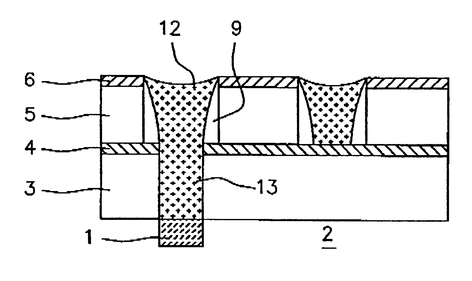
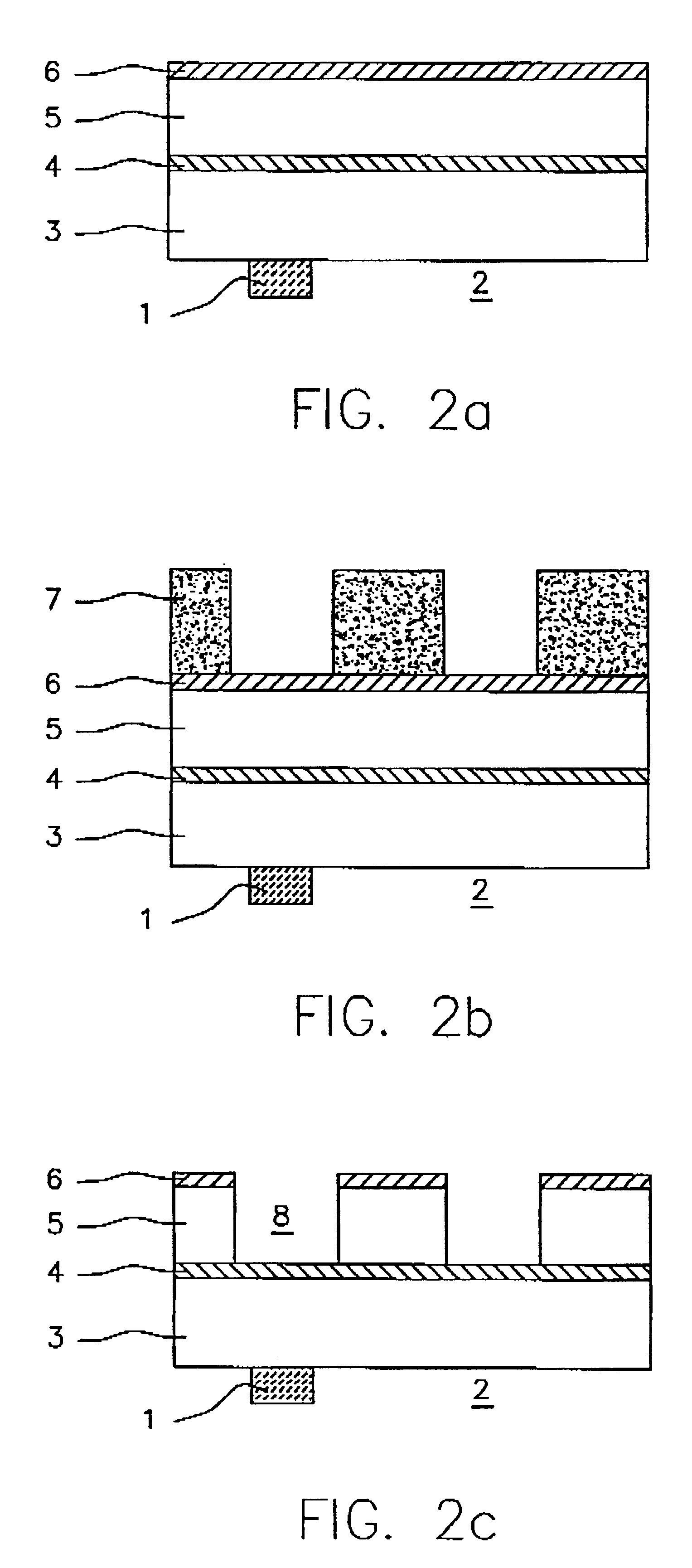
Steps for a novel self aligned dual damascene method according to one embodiment of the present invention are described with reference to FIGS. 2a to 2g. FIG. 2a depicts a step of forming a structure for forming a conductive line and a via plug thereon. The structure is on a first conductive line 1 and a first insulating layer 2 and comprises in a sequence from bottom to top a second insulating layer 3, a first etch stop layer 4, a third insulating layer 5 and a second etch stop layer 6. In the structure, part of the second insulating layer 3 is to be etched and opened for forming a via hole and part of the third insulating layer 5 is to be etched and opened for forming a second conductive line opening. The first etch stop layer 4 between the second and the third insulating layers is used for protecting the second insulating layer 3 from damage of overreaching when etched to form the second conductive line opening. There may be an etch stop layer between the first insulating layer 2...


PUM


Abstract

A method for fabricating an interconnection between a conductive line and a via plug on an insulating layer, comprises the steps of: forming a conductive line pattern on the insulating layer; etching the upper part of the insulating layer and forming a conductive line opening; forming conductive line spacers to provide better alignment between the conductive line and the via, to provide better control of a small via, and to help the metal to have better coverage effects in filling in the conductive line opening and the via; producing a via pattern on the insulating layer and the via pattern opening being substantially larger than the conductive line opening; etching the exposed lower part of the insulating layer by utilizing the conductive line spacers as an etching mask and forming a via hole; and filling the conductive line opening and the via hole with a conductive material and forming an interconnection of the conductive line and a via plug.

Description

BACKGROUND OF THE INVENTION1. Field of the InventionThe present invention relates to a dual damascene method for producing conductive lines and via plugs, and more particularly, to a self aligned dual damascene method for interconnecting metal conductive lines and via plugs in integrated circuits of semiconductor devices so as to connect metal conductive lines in multilayers.2. Description of the Prior ArtAfter producing active and / or passive devices on a semiconductor substrate, metal conductive lines on the devices should be connected. The metal conductive lines are usually laid in multilayer forms. As the integration density of semiconductor devices increases, the interconnection of metal lines in different layers plays an important role and impacts on device performance.The dual damascene method, which mainly deposits and fills metal conductive line openings and via holes between metal conductive lines with a conductive material in one step, is applied to connect metal lines of ...

Claims


Application Information

Patent Timeline
IPC IPC(8): H01L21/768H01L21/70
CPCH01L21/76831H01L21/76807
Inventor CHIEN, WU KUOCHIEH, CHEN HSIPING, CHEN HAN
Owner TAIWAN SEMICON MFG CO LTD
Why Eureka
Try Eureka