Die-based in-fab process monitoring and analysis system for semiconductor processing

a semiconductor and process monitoring technology, applied in the direction of semiconductor/solid-state device testing/measurement, instruments, furnaces, etc., can solve the problems of engendering nonoptimal control of critical processing parameters, many of the processing tools currently commercially available suffer certain deficiencies, and many tools lack advanced process data monitoring capabilities

Inactive Publication Date: 2002-04-09
GLOBALFOUNDRIES INC
View PDF5 Cites 103 Cited by
  • Summary
  • Abstract
  • Description
  • Claims
  • Application Information

AI Technical Summary

Problems solved by technology

However, despite the advances made in this area, many of the processing tools that are currently commercially available suffer certain deficiencies.
In particular, such tools often lack advanced process data monitoring capabilities, such as the ability to provide historical parametric data in a user-friendly format, as well as event logging, real-time graphical display of both current processing parameters and the processing parameters of the entire run, and remote, ie., local site and worldwide, monitoring.
These deficiencies can engender nonoptimal control of critical processing parameters, such as throughput accuracy, stability and repeatability, processing temperatures, mechanical tool parameters, and the like.
However, traditional statistical process control (SPC) techniques are often inadequate to control precisely CDs and doping levels in semiconductor and microelectronic device manufacturing so as to optimize device performance and yield.
Furthermore, blindly minimizing non-adaptive processing spreads about target values may not increase processing yield and throughput.
Traditional control techniques are frequently ineffective in reducing off-target processing and in improving sort yields.
When one or more of the processing steps are producing resulting wafers that WET measurements indicate are unacceptable, causing the resulting wafers to be scrapped, this misprocessing goes undetected and uncorrected for quite a while, often for weeks, leading to many scrapped wafers, much wasted material and decreased overall throughput.
Similarly, process and / or tool problems throughout the wafer processing are typically not analyzed fast enough, and final wafer yields are not evaluated on a die-by-die basis.
Furthermore, data sets for making correlations between processing and / or tool trace data, on the one hand, and testing data, such as WET measurements, on the other, are typically manually extracted by the process engineers and put together, a very time-consuming procedure.

Method used


Image

  • Die-based in-fab process monitoring and analysis system for semiconductor processing
  • Die-based in-fab process monitoring and analysis system for semiconductor processing
  • Die-based in-fab process monitoring and analysis system for semiconductor processing

Examples


exemplary embodiment 2000

the apparatus 1900 in FIG. 19 is illustrated in FIGS. 20-21, in which the apparatus 2000 comprises a portion of an Advanced Process Control ("APC") system. FIGS. 20-21 are conceptualized, structural and functional block diagrams, respectively, of the apparatus 2000. A set of processing steps is performed on a lot of wafers 2005 on a photolithography processing tool 2010. Because the apparatus 2000 is part of an APC system, the wafers 2005 are processed on a run-to-run basis. Thus, process adjustments are made and held constant for the duration of a run, based on run-level measurements or averages. A "run" may be a lot, a batch of lots, or even an individual wafer.

In this particular embodiment, the wafers 2005 are processed by the photolithography processing tool 2010 and various operations in the process are controlled by a plurality of photolithography control input signals on a line 2020 between the photolithography processing tool 2010 and a workstation 2030. Exemplary photolitho...


PUM


Abstract

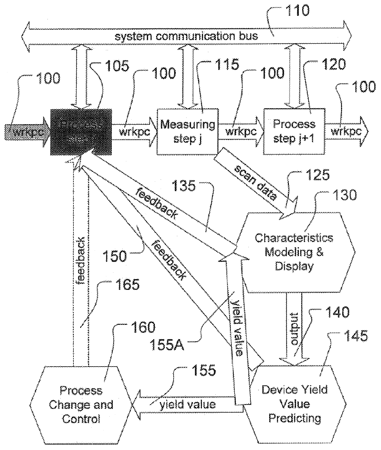
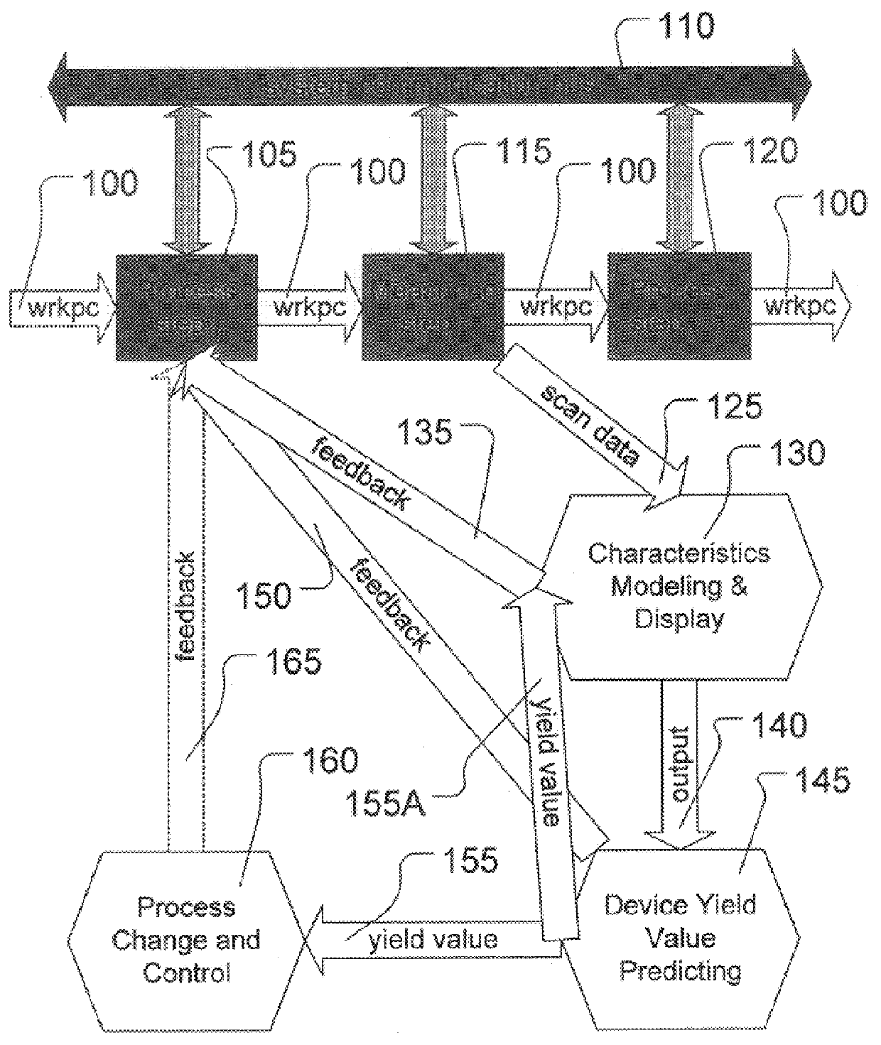
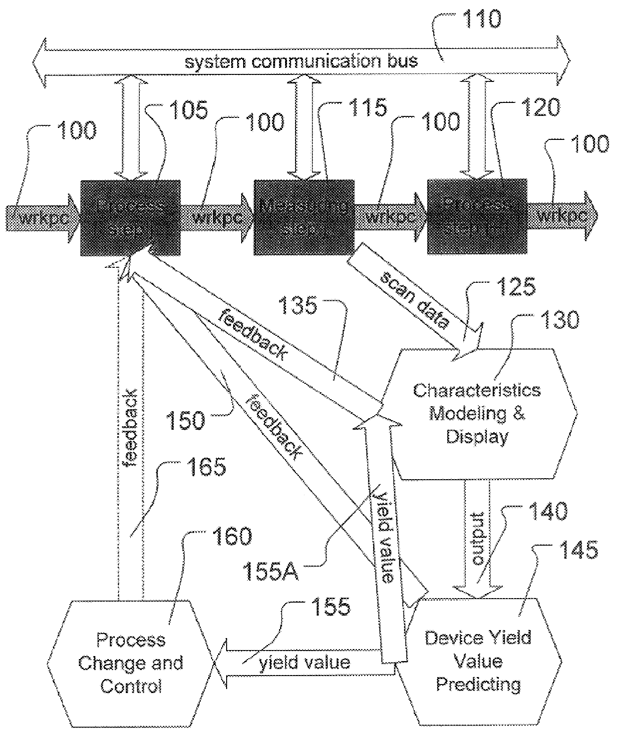
A method is provided for manufacturing, the method including processing a workpiece in a plurality of processing steps and measuring characteristics of the processing performed on the workpiece in at least two of the plurality of processing steps. The method also includes displaying the characteristics measured by overlaying the characteristics measured at each of the at least two of the plurality of processing steps to display a final resulting workpiece.

Description

1. Field of the InventionThis invention relates generally to semiconductor fabrication technology, and, more particularly, to a method for semiconductor fabrication supervision and optimization.2. Description of the Related ArtThere is a constant drive within the semiconductor industry to increase the quality, reliability and throughput of integrated circuit devices, e.g., microprocessors, memory devices, and the like. This drive is fueled by consumer demands for higher quality computers and electronic devices that operate more reliably. These demands have resulted in a continual improvement in the manufacture of semiconductor devices, e.g., transistors, as well as in the manufacture of integrated circuit devices incorporating such transistors. Additionally, reducing defects in the manufacture of the components of a typical transistor also lowers the overall cost per transistor as well as the cost of integrated circuit devices incorporating such transistors.The technologies underlyi...

Claims


Application Information

Patent Timeline
Patent Type & Authority Patents(United States)
IPC IPC(8): H01L21/66
CPCH01L22/20H01L2223/5448
Inventor GOODWIN, GREGOSHELSKI, ANASTASIA LYNN
Owner GLOBALFOUNDRIES INC
Why Eureka
Try Eureka