
Quantum magnetic memory

a magnetic memory and quantum technology, applied in the field of memory systems, can solve the problems of processing starving for data, difficult to alter the magnetic properties of the magnetic properties, and limited data transfer

Inactive Publication Date: 2002-05-14
INTEL CORP
View PDF4 Cites 20 Cited by
  • Summary
  • Abstract
  • Description
  • Claims
  • Application Information

AI Technical Summary

Benefits of technology

The present invention has been illustrated using specific embodiments. Persons skilled in the art and having the benefit of this disclosure will recognize that these embodiments are subject to a variety of modifications that none the less fall within the spirit and scope of the appended claims.

Problems solved by technology

Data transfer is limited by the speed at which the disc rotates and the speed with which the read / write head is positioned over the required track.
The discrepancy can leave the processor starved for data.
One problem with the disclosed system is that the characteristics of the storage media that provide desirable magnetic properties also make it difficult to alter these magnetic properties, i.e. a magnetic material, such as iron (Fe), deposited on a layer of a conductive, non-magnetic material.
An additional problem is that electron beam sources produce electron energies of several tens of electron volts (eV).
The combination of the thin layer of magnetic material, the normally incident beam, and the high electron energy thus limits the strength of the coupling between the spin-polarized electron beam and the target electrons.
The STM geometry and physical translation mechanism are not suitable for high performance storage media applications.
For example, the close proximity of the scanning tip to the surface limits the area of the storage medium that may be scanned by deflecting the electron beam.
In addition, STM scanning techniques translate the entire STM apparatus relative to the medium, making them too slow for processor applications.

Method used


Image

  • Quantum magnetic memory
  • Quantum magnetic memory
  • Quantum magnetic memory

Examples


Embodiment Construction

The following discussion sets forth numerous specific details to provide a thorough understanding of the invention. However, those of ordinary skill in the art, having the benefit of this disclosure, will appreciate that the invention may be practiced without these specific details. In addition, various well-known methods, procedures, components, and circuits have not been described in detail in order to focus attention on the features of the present invention.

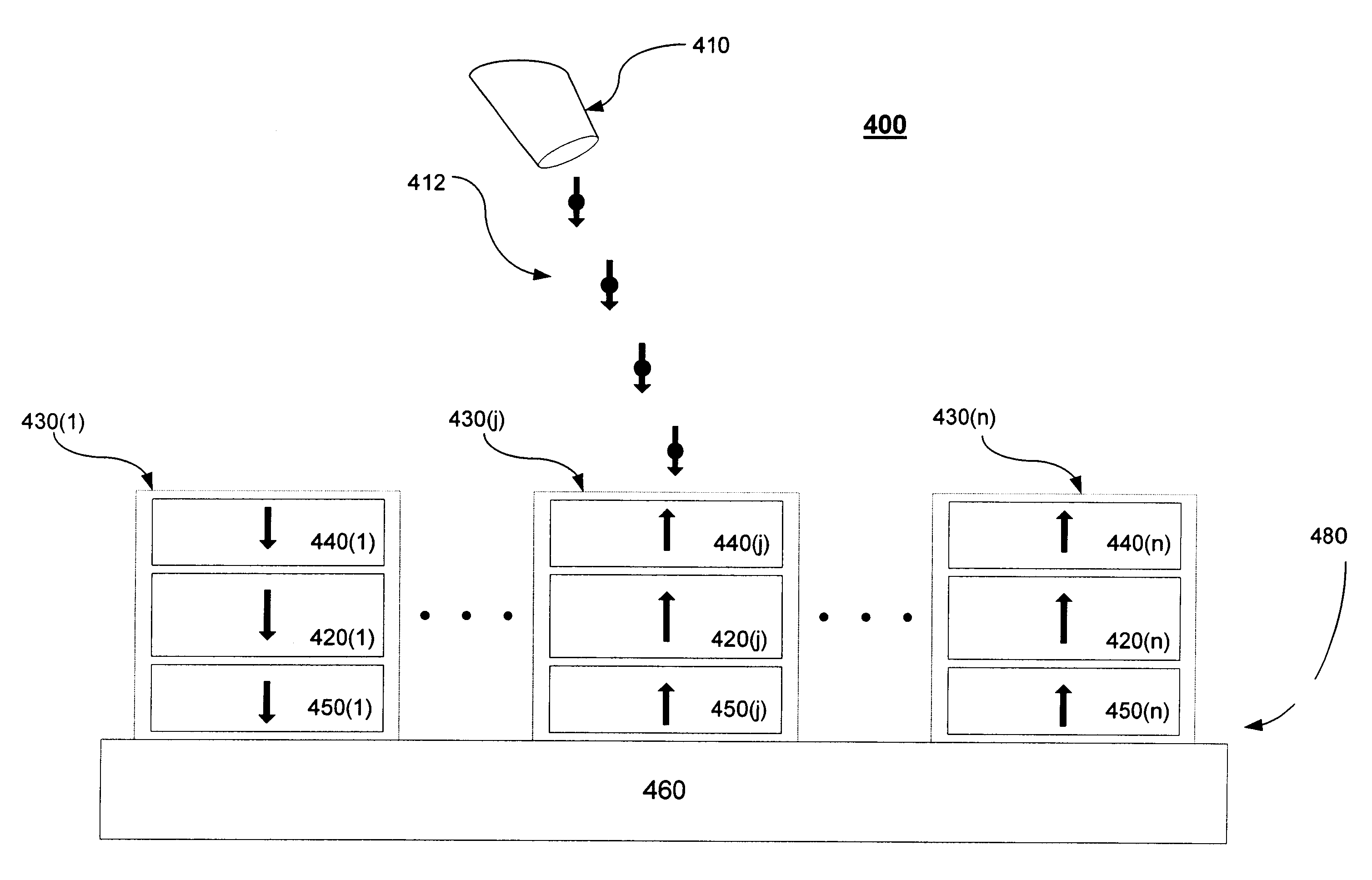
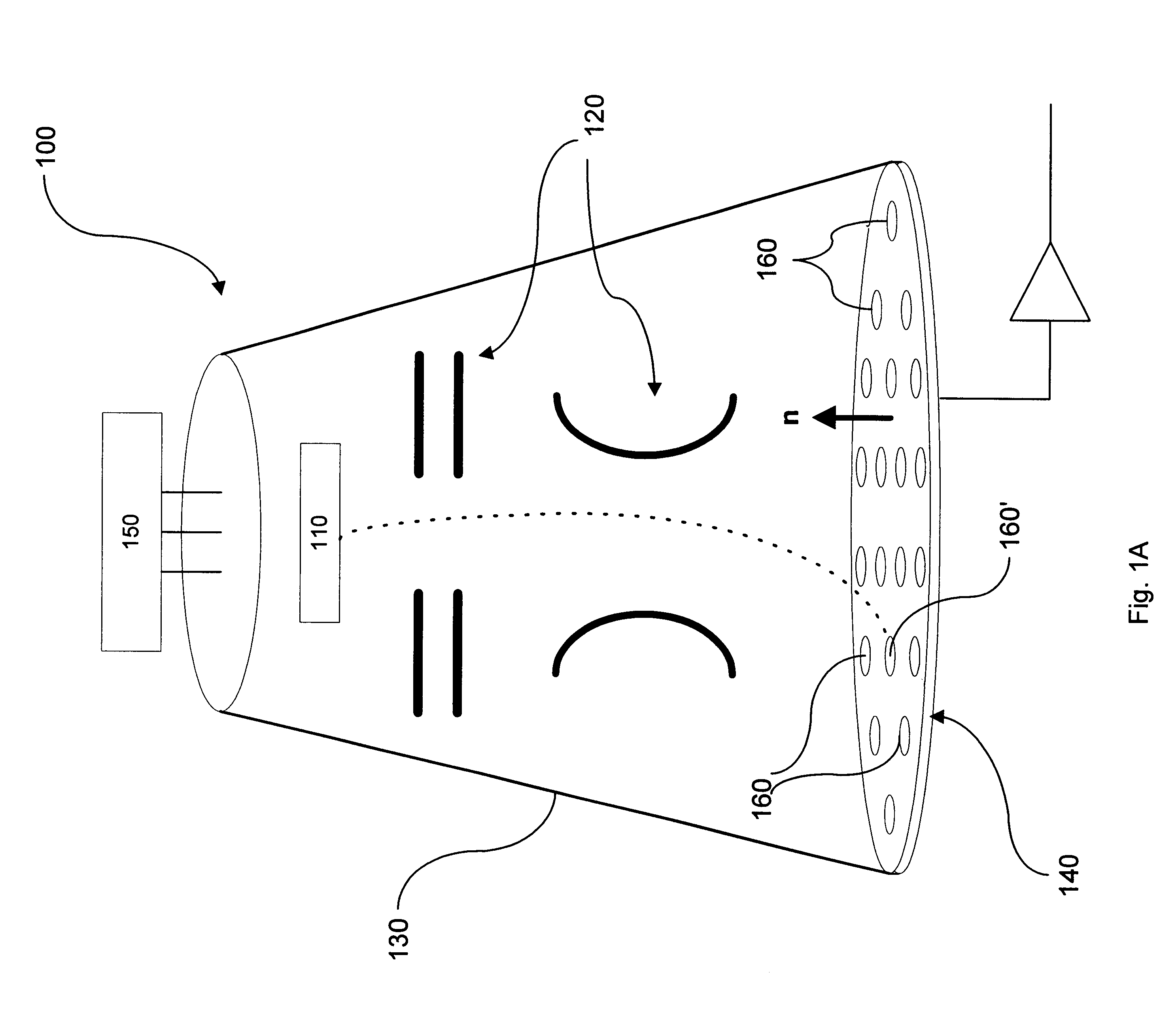
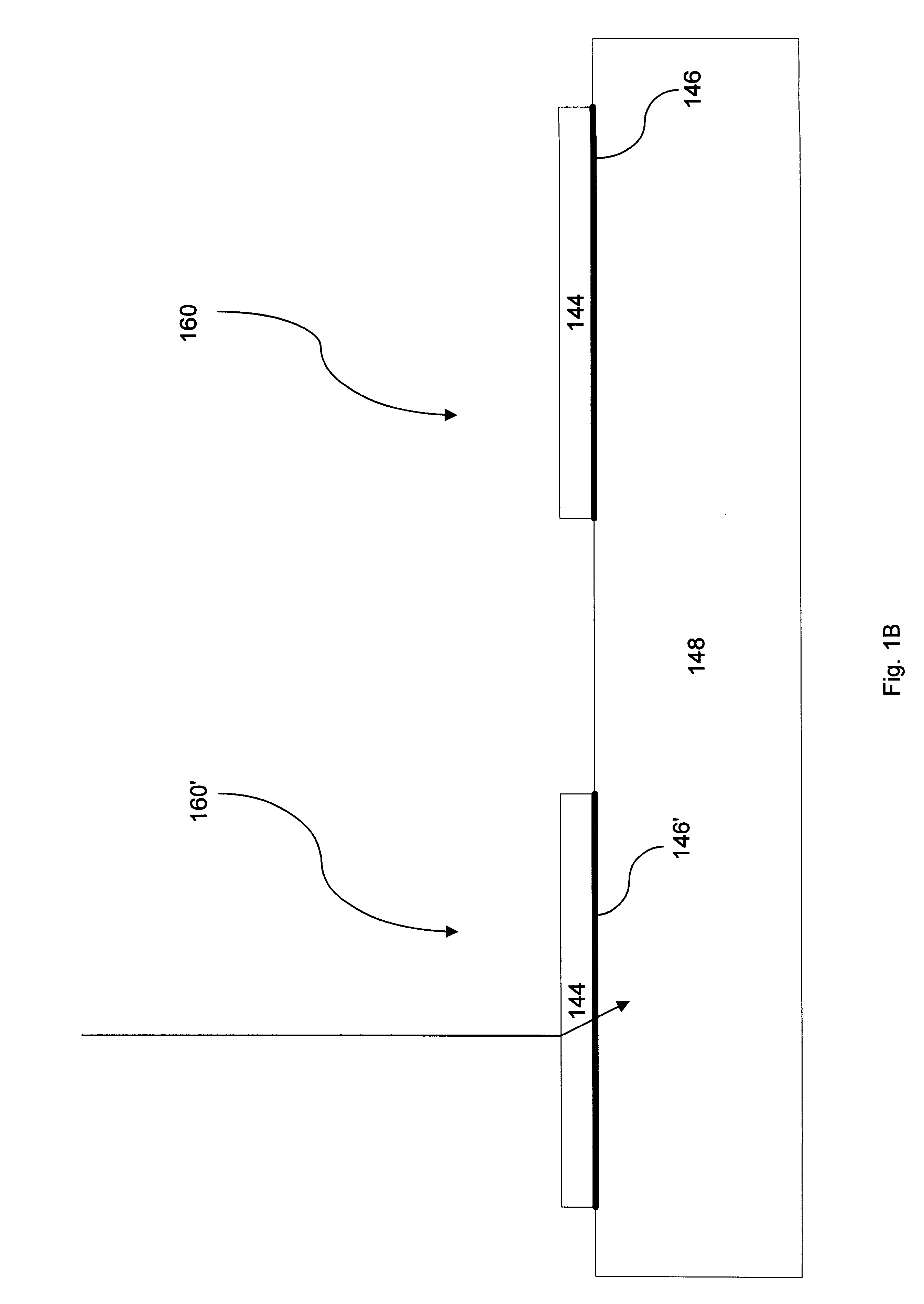
The present invention provides a system for reading data from and writing data to a storage medium, using a beam of spin-polarized electrons. A system in accordance with the present invention employs a storage medium that promotes enhanced coupling between the spin-polarized electrons of the beam ("beam electrons") and the electrons of a magnetic layer in the storage medium ("target electrons"). Beam electrons of a particular spin polarization are preferentially trapped in a volume that includes the magnetic layer, allowing ea...


PUM


Abstract

A system for storing data on a magnetic medium using spin polarized electron beams is provided. The system includes a source of spin polarized electrons and a storage medium disposed a selected distance from the source. The storage medium has a plurality of storage locations, each of which includes a layer of magnetic material sandwiched between first and second layers of a half-metallic material. The resulting sandwich structure forms a spin dependent electron trap that increases coupling between beam electrons in a first spin state and target electrons in a second spin state. An electron optics system directs the source of spin polarized electrons to one of the plurality of storage locations.

Description

1. Technical FieldThe present invention relates to memory systems and in particular to systems and methods for writing data to magnetic memory systems using spin-polarized electron beams.2. Background ArtThe predominant mass storage device in conventional computer system is the hard disk drive. Hard disk drives are relatively large, electromechanical devices that can store tens of gigabits of data. The stored data is accessed through a read / write head that rides on a cushion of air above the rapidly rotating disk. The read / write head moves radially to access data in different tracks of the rotating disk. Data transfer is limited by the speed at which the disc rotates and the speed with which the read / write head is positioned over the required track. Even with the fastest devices, access times are on the order of thousands of microseconds, due to the relatively large mechanical motions and inertia involved. This time scale is at least five orders of magnitude slower than the nanoseco...

Claims


Application Information

Patent Timeline
IPC IPC(8): G11B11/00G11B11/11G11B11/115G11B5/00H01F10/32G11C11/16G11C11/02H01F10/00
CPCB82Y25/00G11B5/00G11B11/11H01F10/32G11C11/16G11B11/115G11B2005/0002G11C11/161G11C11/1675G11B9/10
Inventor HANNAH, ERIC C.BROWN, MICHAEL
Owner INTEL CORP
Learn More