Semiconductor device

a technology of semiconductor devices and bumps, applied in semiconductor devices, semiconductor/solid-state device details, electrical apparatus, etc., can solve problems such as affecting reliability, weak connection between bumps and lands disclosed, etc., to reduce the size of bumps, increase the number of bumps, and reduce the pitch

Inactive Publication Date: 2002-05-28
NEC ELECTRONICS CORP
View PDF22 Cites 38 Cited by
  • Summary
  • Abstract
  • Description
  • Claims
  • Application Information

AI Technical Summary

Benefits of technology

It is expected that a semiconductor device with a semiconductor package will have more pins as the semiconductor chip have more electrode pads. To cope with the incr

Problems solved by technology

The reduction in the pad-to-pad pitch and in the bump size to accommodate more pins results in a weak connection between the bumps and the lands disclosed on the insulation film.
In ad

Method used


Image

  • Semiconductor device
  • Semiconductor device
  • Semiconductor device

Examples


examples

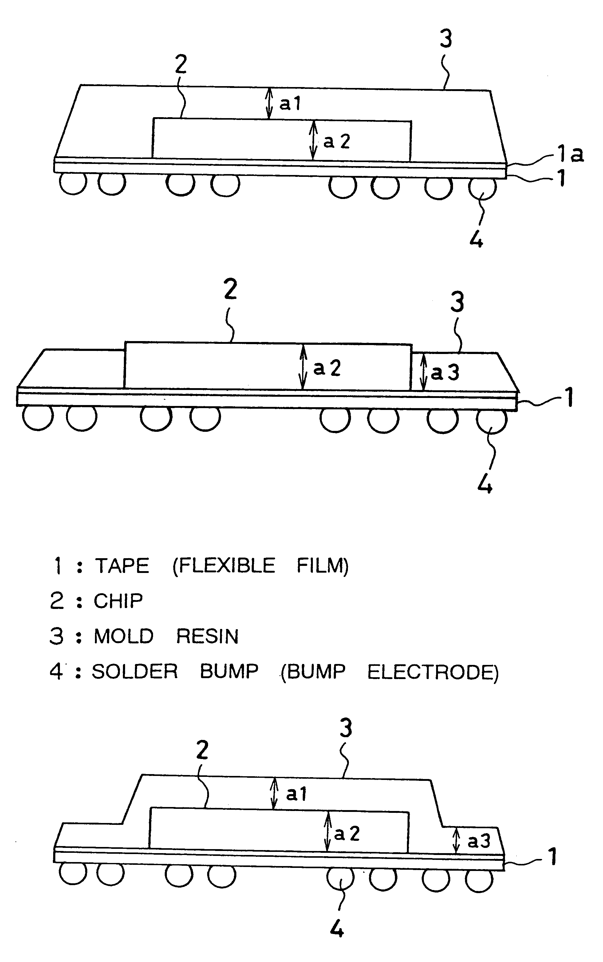
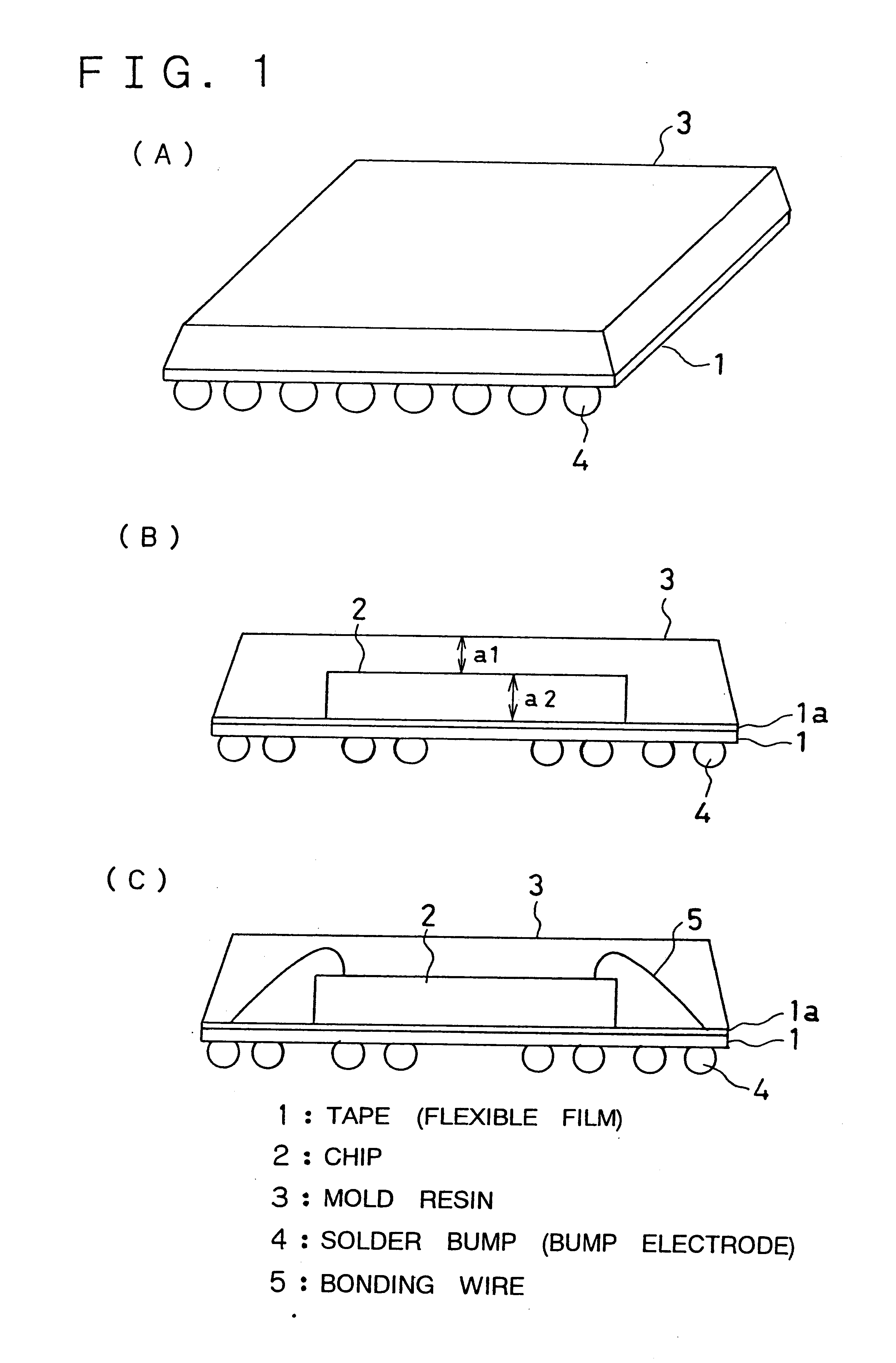
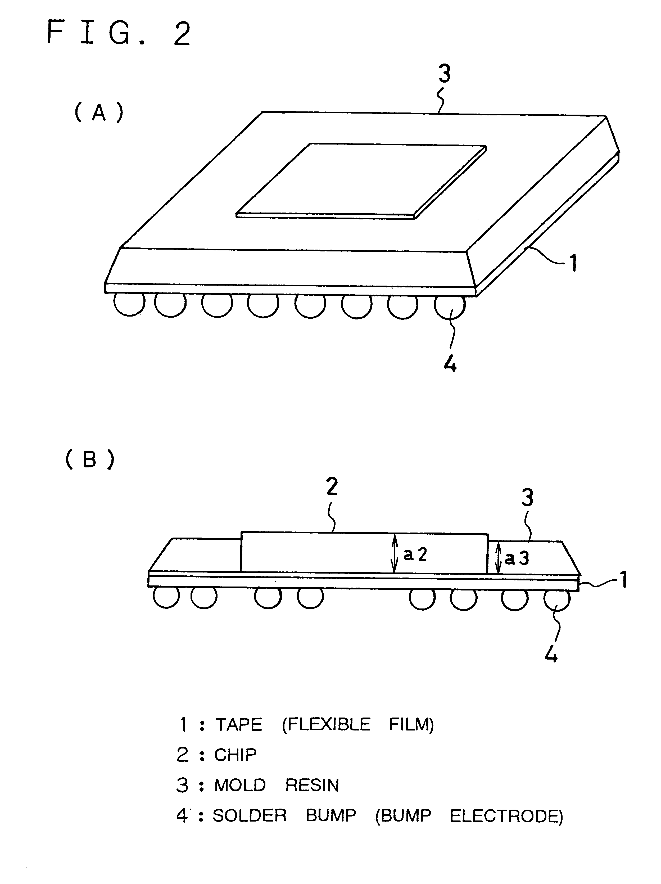
The embodiments of the various aspects of the present invention given above will be described more in more detail by way of examples referring to the drawings. Semiconductor devices used in the embodiments explained with reference to FIGS. 1 and 2 were mounted on a substrate, and the following reliability test (temperature cycle test) was made. The test result is shown in FIG. 5.

Temperature cycle condition: -25.degree. C.-to 125.degree. C. (10 minutes at low temperature, 10 minutes at high temperature)

In FIG. 5, a semiconductor device whose "thickness of the mold on the top of the chip" is 0 .mu.m or larger is the semiconductor device shown in FIG. 1 (B). With a2 (thickness of the semiconductor chip) fixed to 350 .mu.m, various samples were created by changing al (thickness of the mold resin on the top of the chip) a s follows: 500 .mu.m, 400 .mu.m, 300 .mu.m, 150 .mu.m, and 0 .mu.m. The temperature cycle test was made with these semiconductor devices on the substrate. The vertical ...


PUM


Abstract

A semiconductor device which eliminates a thermal stress in the semiconductor device or warp in a package of the semiconductor device to increase reliability. To achieve this, the semiconductor device has a structure in which an insulation flexible film and a semiconductor chip are stuck together. The insulation flexible film has on the obverse side a plurality of electrode pads and, on the reverse side, a plurality of electrodes electrically connected to the plurality of electrode pads. The semiconductor chip is sealed on the chip-mounting side of the insulation flexible film with resin, with a thickness of the resin above the semiconductor chip equal to or less than the thickness of the semiconductor chip.

Description

The present invention relates to a semiconductor device, and more particularly to a package structure that may be applied to a chip size package (hereafter called "CSP"), fine pitch ball grid array (hereafter called "FBGA"), and so forth.A ball grid array (BGA) package and a land grid array (LGA) have been known as the package structure of a semiconductor device. For a semiconductor with this structure, the chip carrier, which contains a semiconductor, has external electrode pads arranged on a grid on one side of the package. As compared with a quad flat package (QFP), this semiconductor device is greatly reduced in size because it has the external electrode pads on one side of the package. In addition, the pin-to-pin pitch, 1.5 mm or 1.27 mm, is relatively large as compared with that of a QFP which is 0.3 mm or 0.5 mm, making installation easier. Thanks to these advantages, BGA and LGA packages have been accepted as new semiconductor devices.To make the package further smaller and ...

Claims


Application Information

Patent Timeline
IPC IPC(8): H01L23/31H01L23/16H01L23/28H01L23/433H01L23/34H01L23/12H01L21/60
CPCH01L23/16H01L23/31H01L23/3128H01L23/4334H01L2224/48227H01L2924/01087H01L2924/15311H01L2924/1815H01L2924/3511H01L24/48H01L2924/01079H01L24/45H01L2224/45144H01L2924/00014H01L2924/181H01L2224/05599H01L2224/85399H01L2224/45015H01L2924/207H01L2924/00012H01L23/12
Inventor SHOJI, KAZUTAKA
Owner NEC ELECTRONICS CORP
Why Eureka
Try Eureka