Conditional clock buffer circuit
a buffer circuit and clock technology, applied in the field of electronic circuits, can solve the problems of reducing power consumption of functional logics receiving output clock signals, increasing power consumption,
- Summary
- Abstract
- Description
- Claims
- Application Information
AI Technical Summary
Problems solved by technology
Method used
Image
Examples
Embodiment Construction
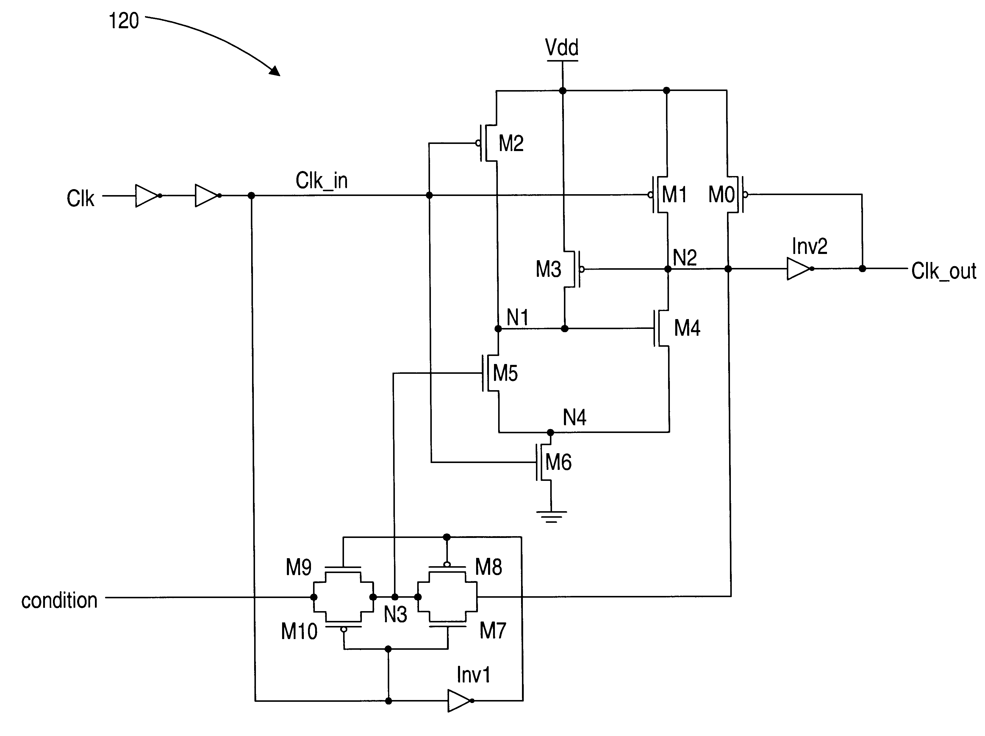
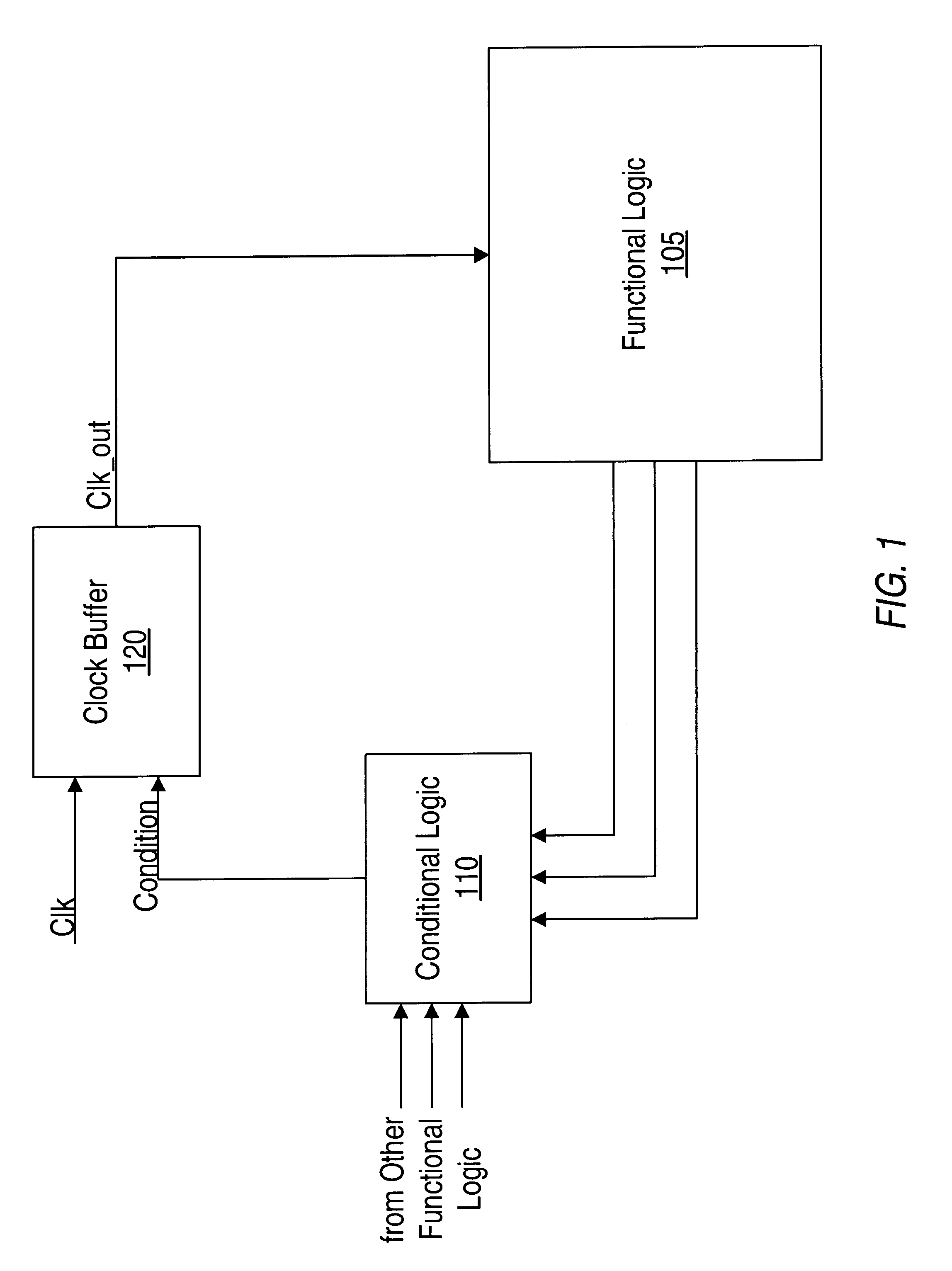
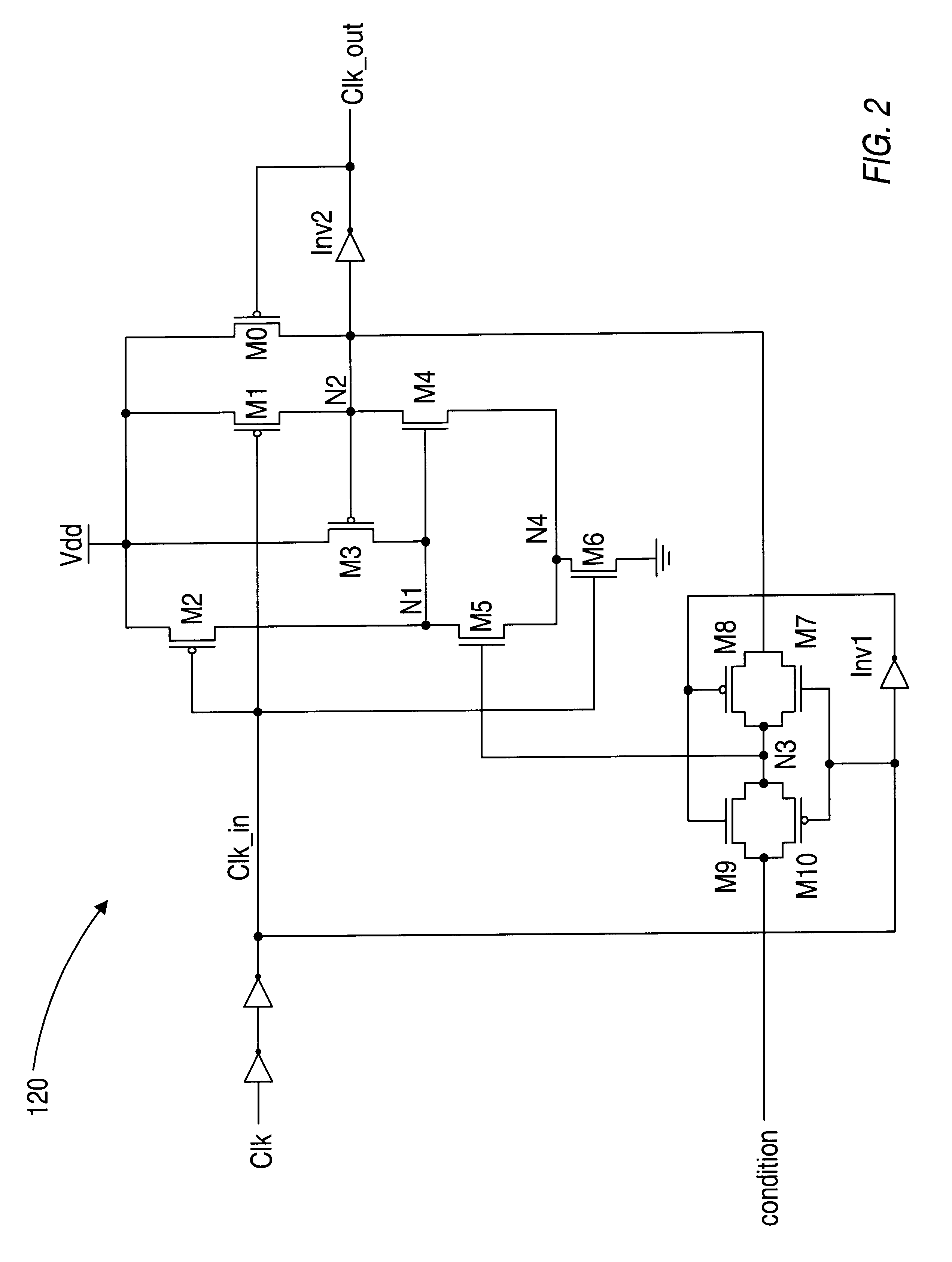
Turning now to FIG. 1, a block diagram of a circuit in which one embodiment of a clock buffer circuit 120 may be implemented is shown. In the embodiment shown, clock buffer circuit 120 is a conditional clock buffer circuit, and is configured to receive an input clock signal, Clk, and drive an output clock signal, Clk.sub.13 out, to functional logic 105. Functional logic 105 may be any type of clocked logic circuit. In various embodiments, functional logic 105 may be an integrated circuit, or a portion of an integrated circuit. Some integrated circuits may include a plurality of clock buffers 120, each having an associated conditional logic 110 and an associated functional logic 105. Employing multiple instances of clock buffer 120 and conditional logic 110 in an integrated circuit may allow for fine grain power management.
Conditional logic 110 may be coupled to functional logic 105. Conditional logic 110 may monitor operation in functional logic 105 and / or other logic coupled to the...
PUM
 Abstract
Description
Claims
Application Information


