

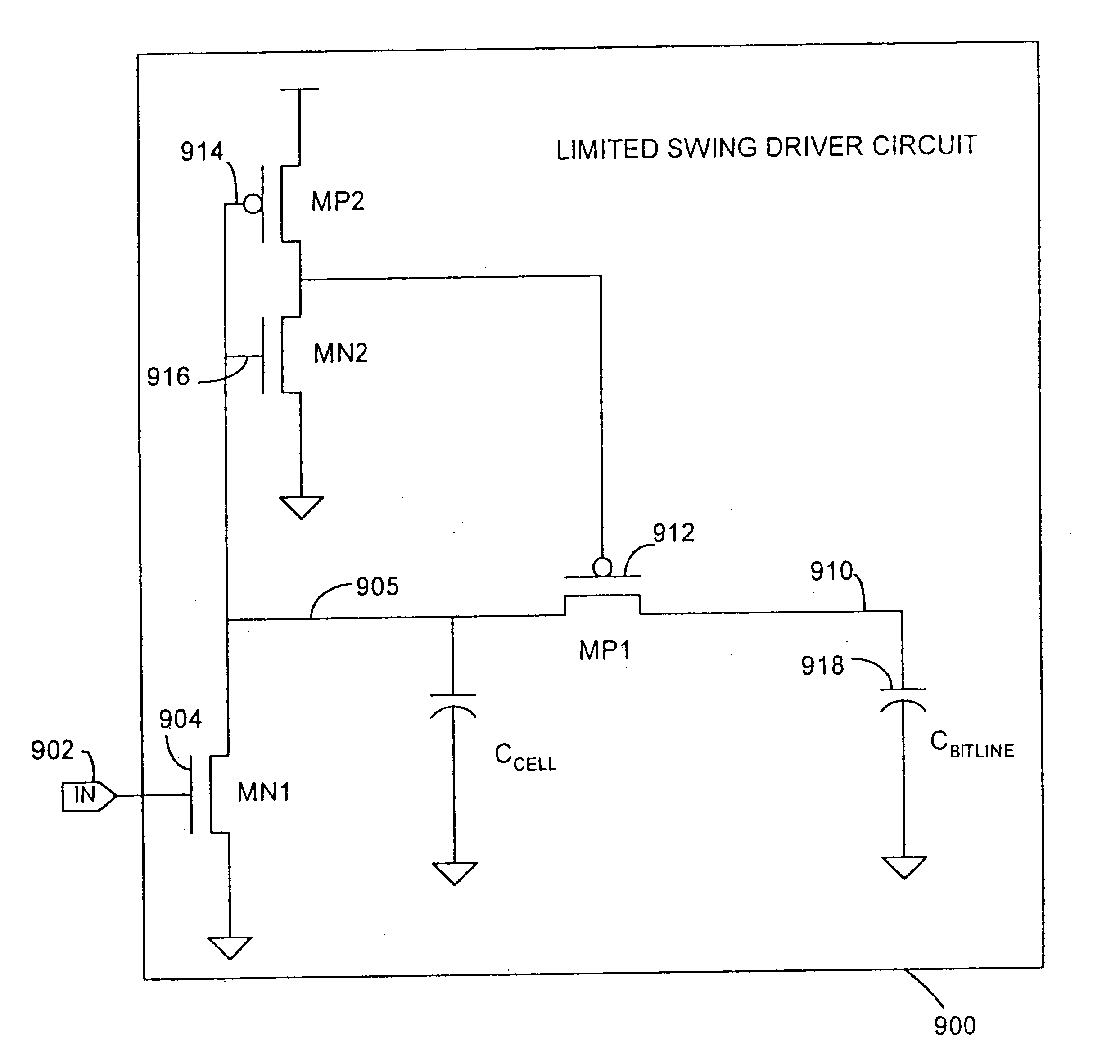
Limited swing driver circuit
a technology of swing driver and circuit, applied in the field of memory devices, can solve the problems of limiting, or even precluding, the scalability of the sram subsystem design, and the specific adaptions of the sram subsystem,
- Summary
- Abstract
- Description
- Claims
- Application Information
AI Technical Summary
Benefits of technology
Problems solved by technology
Method used
Image

Examples
Embodiment Construction
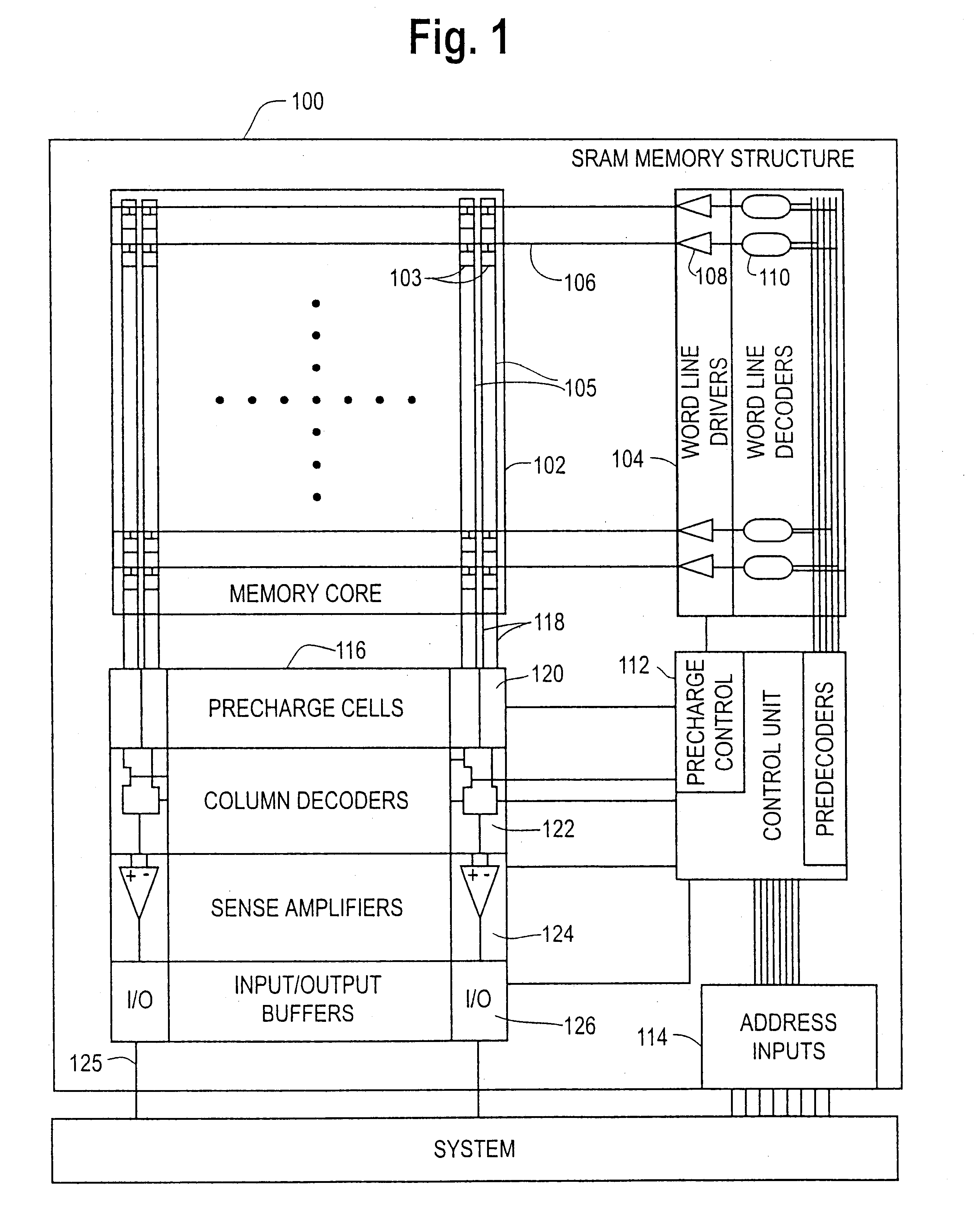
As will be understood by one having skill in the art, most VLSI systems, including communications systems and DSP devices contain VLSI memory subsystems. Modern applications of VLSI memory subsystems almost invariably demand high efficiency, high performance implementations that magnify the design tradeoff between layout efficient, speed, power consumption, scalability, design tolerances, and the like. The present invention ameliorates these tradeoffs using a novel hierarchical architecture. The memory module of the present invention also can employ one or more novel components which further add to the memory modules efficiency and robustness.
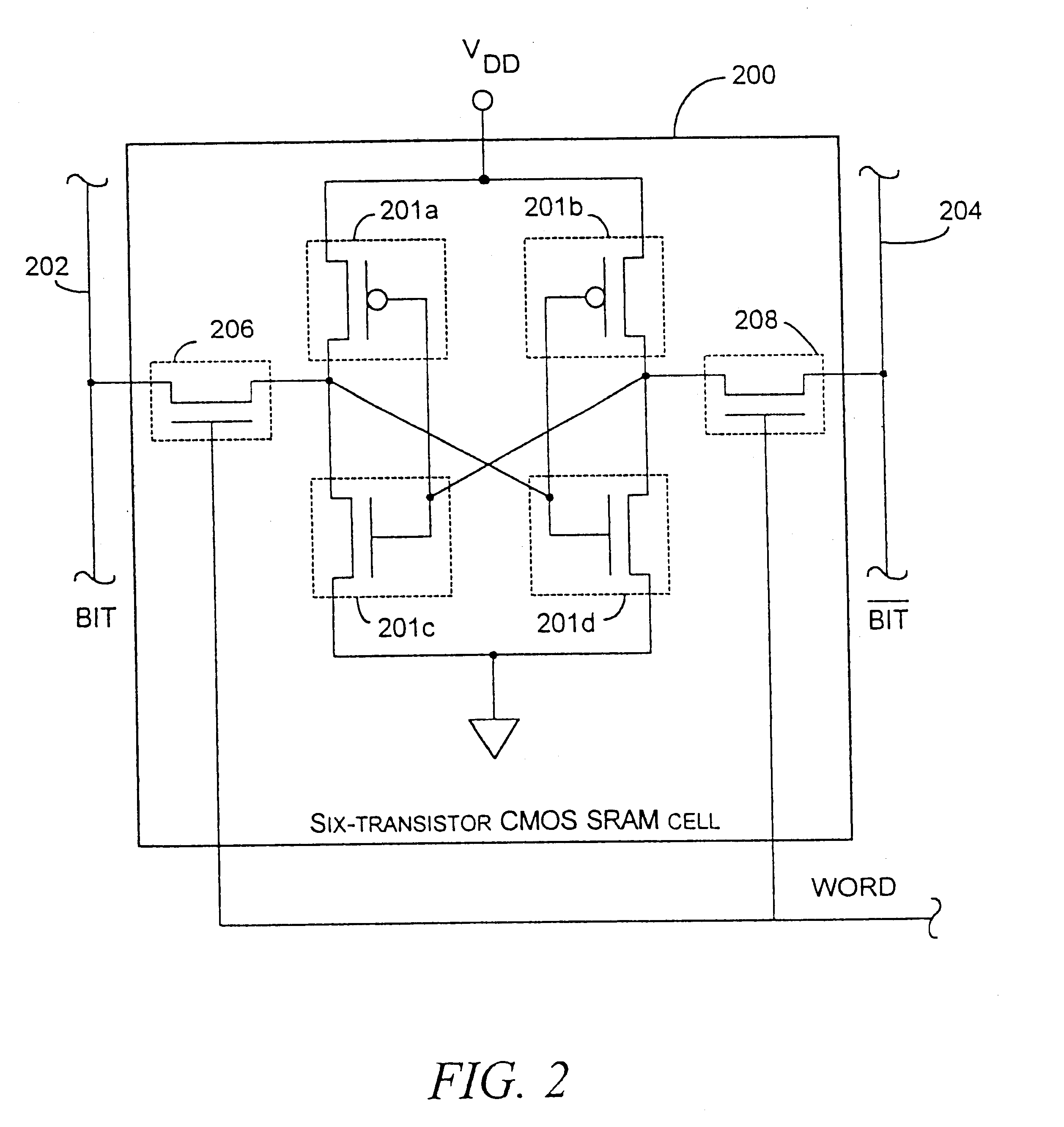
Hereafter, but solely for the purposes of exposition, it will be useful to describe the various aspects and embodiments of the invention herein in the context of an SRAM memory structure, using CMOS SRAM memory cells. However, it will be appreciated by those skilled in the art the present invention is not limited to CMOS-based processes and tha...
PUM
 Abstract
Description
Claims
Application Information