High voltage level shifter for switching high voltage in non-volatile memory integrated circuits

a technology of high voltage and integrated circuit, which is applied in the direction of electronic switching, pulse automatic control, pulse technique, etc., can solve the problems of increasing the operating current of the circuit, circuit malfunction, and incompatibility of the voltage range over which a signal swings, so as to improve the gated diode breakdown of the nmos device, the effect of high junction breakdown of the n+ drain

Inactive Publication Date: 2002-08-20
WINBOND ELECTRONICS CORP
View PDF4 Cites 49 Cited by
  • Summary
  • Abstract
  • Description
  • Claims
  • Application Information

AI Technical Summary

Benefits of technology

A high voltage level shifter utilizing only low voltage PMOS and low voltage NMOS devices. The high voltage level shifter is used to distribute the high voltage almost equally among the PMOS devices and almost equally among the NMOS devices to meet the device electrical specification of low voltage MOS devices for various breakdown mechanisms. A layout technique is also used to achieve a much higher junction breakdown of N+ drain to P-substrate and a better gated diode breakdown of NMOS devices.

Problems solved by technology

However, the voltage range over which a signal swings is often incompatible with other sections of the circuit.
In the case of CMOS integrated circuits, violation of the logic signals may result in malfunction of the circuit due to unrecognizable logic signal levels, and also in simultaneous conduction of PMOS and NMOS devices, thereby increasing the operating current of the circuit.
Signals generated from a higher supply than the circuit to be controlled may also cause malfunction.
Such special high voltage steps are generally undesirable.

Method used


Image

  • High voltage level shifter for switching high voltage in non-volatile memory integrated circuits
  • High voltage level shifter for switching high voltage in non-volatile memory integrated circuits
  • High voltage level shifter for switching high voltage in non-volatile memory integrated circuits

Examples


Embodiment Construction

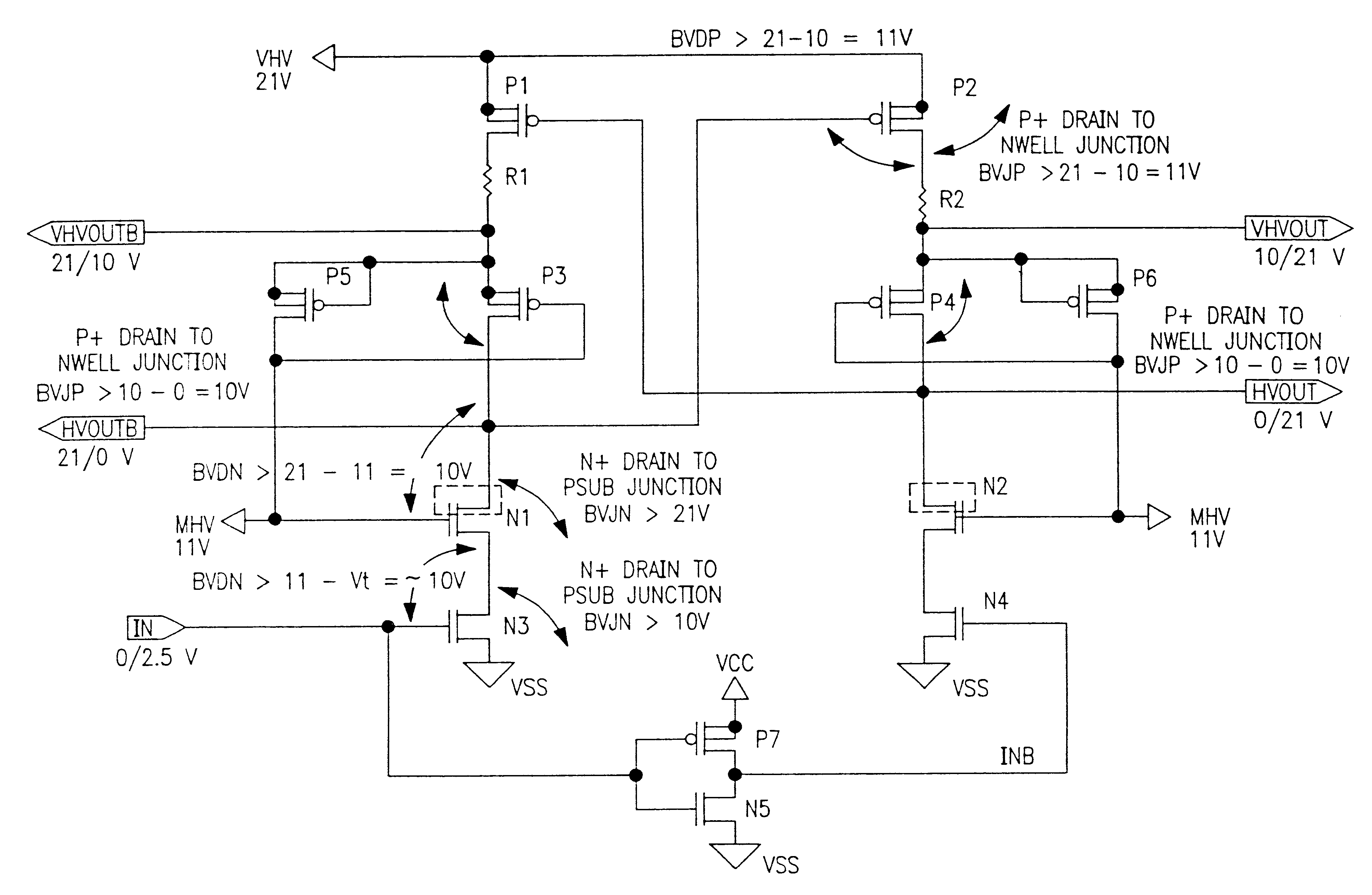
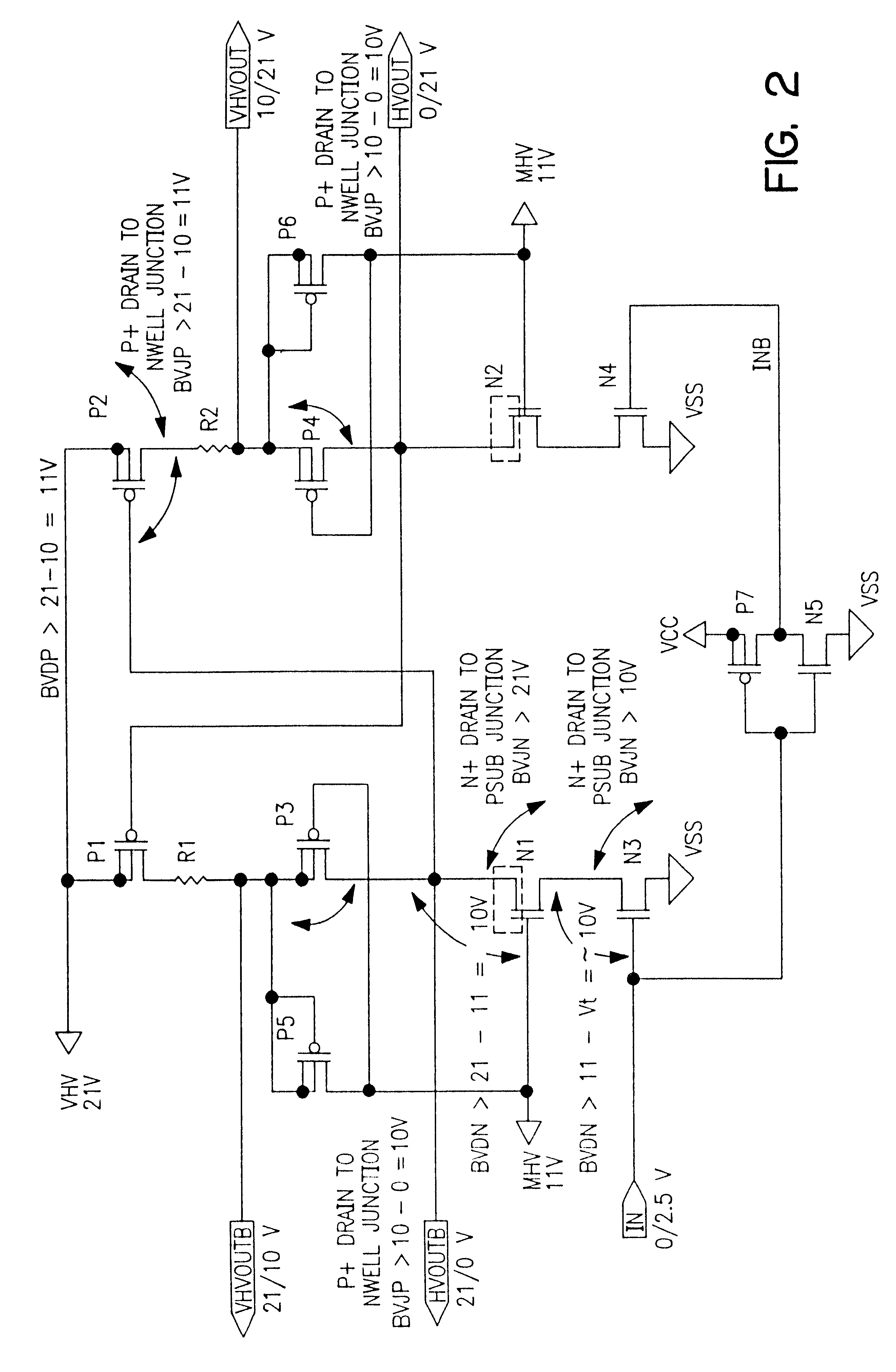
A method and apparatus for a high voltage level shifter utilizing only low voltage P-channel and N-channel devices is described.

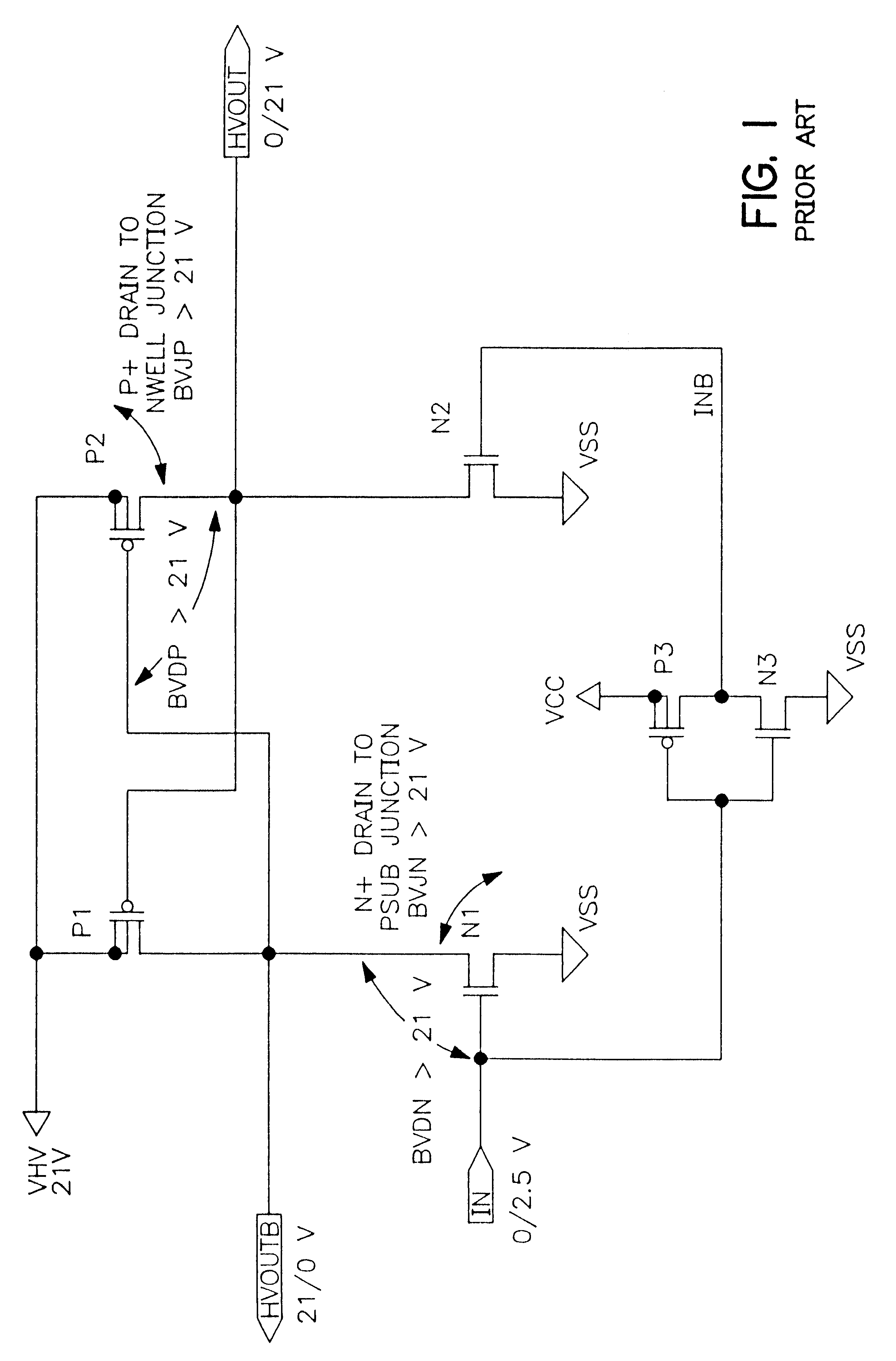
FIG. 2 is a circuit diagram for a preferred embodiment of the present invention. In this circuit, the P-channel devices are labeled as P1, P2, P3, P4, P5, P6 and P7 respectively. Similarly, the N-channel devices are labeled N1, N2, N3, N4 and N5 respectively. A very high voltage source, VHV, is the operating high voltage, in the preferred embodiment typically 21 volts. A medium high voltage source, MHV, is an intermediate level shift voltage, in the preferred embodiment typically 11 volts. A third voltage source, VSS, is the operating low voltage, in the preferred embodiment typically 0 volts. The input signal IN has an input voltage either equal to VSS or a level above VSS. However, in another embodiment, the input signal may be referenced to VHV and is either equal to VHV or a level below VHV. Referring again to FIG. 2, HVOUT and HVOUTB are complementary ...


PUM


Abstract

A high voltage level shifter utilizing only low voltage PMOS and low voltage NMOS devices. The high voltage level shifter is used to distribute the high voltage almost equally among the PMOS devices and almost equally among the NMOS devices to meet the device electrical specification of low voltage MOS devices for various breakdown mechanisms. A layout technique is also used to achieve a much higher junction breakdown of N+ drain to P-substrate and a better gated diode breakdown of NMOS devices.

Description

1. Field of the InventionThe present invention relates to the field of CMOS Integrated Circuits, specifically circuits for switching high voltages on chip in non-volatile memory integrated circuits.2. Prior ArtIntegrated circuits which operate with two or more power supplies invariably require signals to interface between sections of the circuit supplied by different power supply voltages. Multiple power supply voltages may be supplied from external power sources, or, in the case of several classes of integrated circuits such as non-volatile memories, watch circuits and display drivers, may be generated internally or on-chip from a single power source. However, the voltage range over which a signal swings is often incompatible with other sections of the circuit. For example, logic signals with a smaller voltage swing than the circuits to be controlled, may violate the maximum low levels or minimum high levels required by said circuits. In the case of CMOS integrated circuits, violat...

Claims


Application Information

Patent Timeline
Patent Type & Authority Patents(United States)
IPC IPC(8): H03K3/00H03K17/10H03K3/356H03K19/0185
CPCH03K3/356052H03K3/356147H03K17/102H03L5/00
Inventor TRAN, HIEU VANBLYTH, TREVOR
Owner WINBOND ELECTRONICS CORP
Why Eureka
Try Eureka