Optical waveguide structures
- Summary
- Abstract
- Description
- Claims
- Application Information
AI Technical Summary
Problems solved by technology
Method used
Image
Examples
Embodiment Construction
OF APPLICATION
Examples of practical waveguide structures and integrated optics devices which can be implemented using the invention will now be described with reference also to FIGS. 17 to 33.
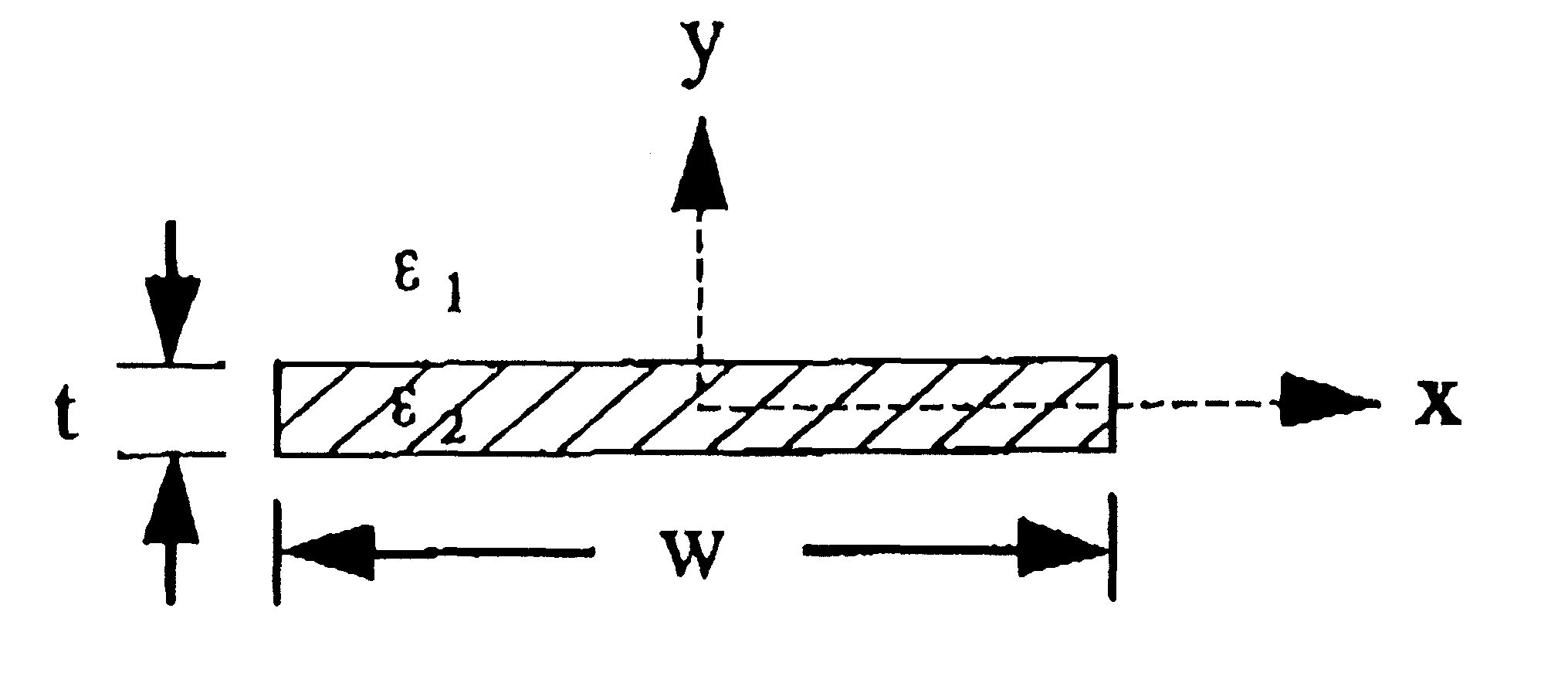
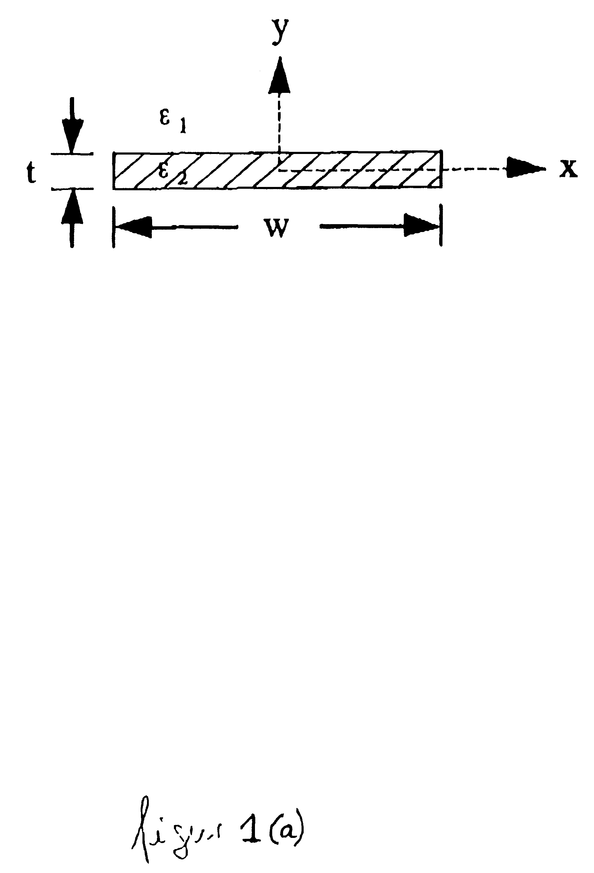
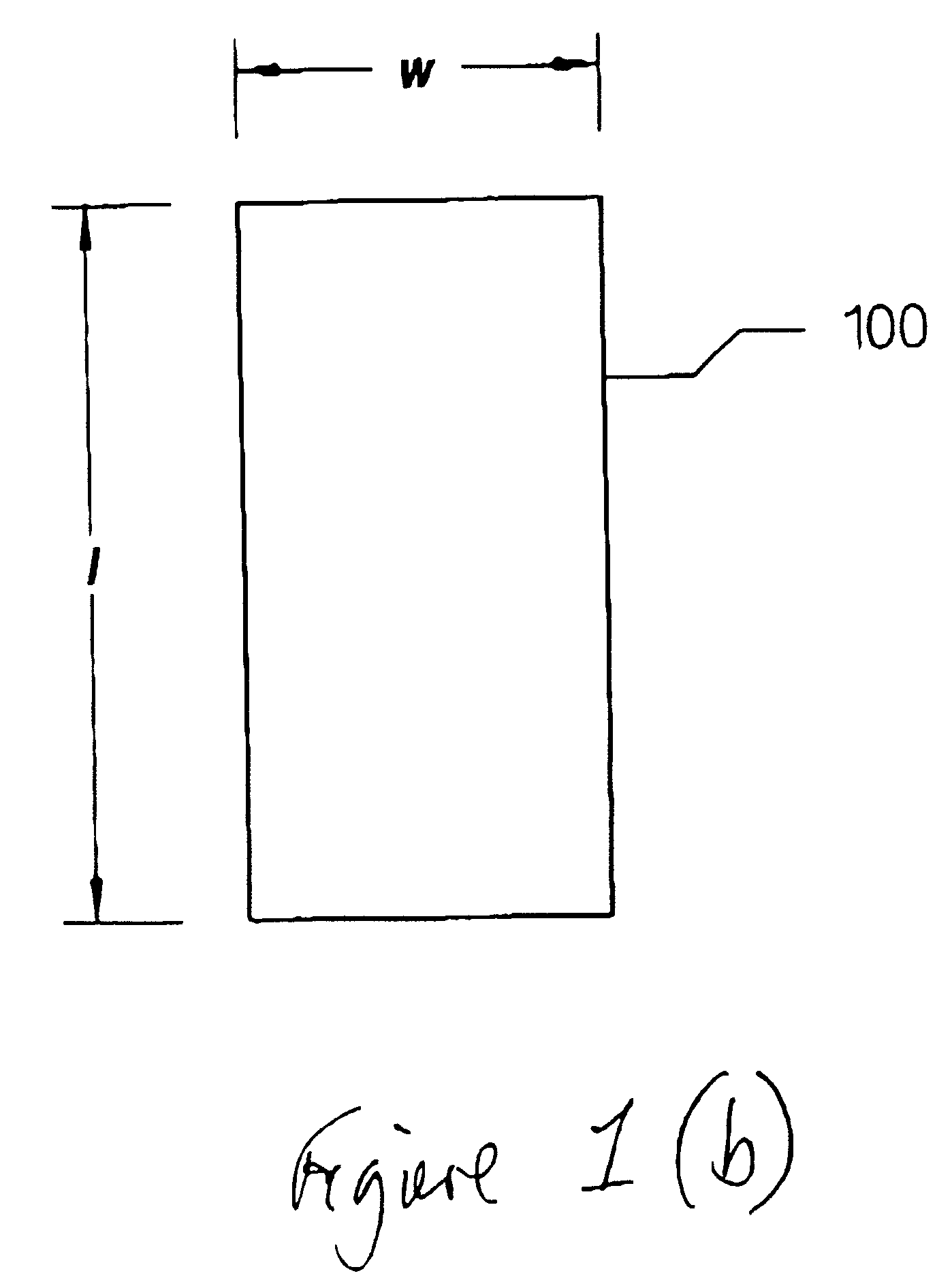
The waveguide structure 100 shown in FIGS. 1(a) and 1(b) comprises a strip of finite thickness and width of a first material having a high free (or almost free) charge carrier density, surrounded by a second material which has a very low free carrier density. The strip material can be a metal or a highly doped semiconductor and the background material can be a dielectric.
Suitable materials for the strip include (but are not limited to) gold, silver, copper, aluminium and highly n- or p-doped GaAs, InP or Si, while suitable materials for the surrounding material include (but are not limited to) glass, quartz, polymer and undoped or very lightly doped GaAs, InP or Si. Particularly suitable combinations of materials include Au for the strip and SiO.sub.2 for the surrounding material.
The thickness ...
PUM
 Abstract
Description
Claims
Application Information


