Method for vertically integrating active circuit planes and vertically integrated circuit produced using said method

a technology of active circuit planes and vertical integration, which is applied in the direction of basic electric elements, electrical apparatus, semiconductor devices, etc., can solve the problems that the thickness dimension cannot be used in a sensible way, and the method is only suitable for components with a small number of terminals, and not for logic units with a large number of terminals

Inactive Publication Date: 2002-09-03
S AQUA SEMICONDUCTOR LLC
View PDF17 Cites 13 Cited by
  • Summary
  • Abstract
  • Description
  • Claims
  • Application Information

AI Technical Summary

Problems solved by technology

Hence, such a utilization of the thickness dimension cannot be realized in a sensible way.
These methods are, however, only suitable for components having a small number of terminals, e.g. for storage components, but not for logic unit

Method used


Image

  • Method for vertically integrating active circuit planes and vertically integrated circuit produced using said method
  • Method for vertically integrating active circuit planes and vertically integrated circuit produced using said method
  • Method for vertically integrating active circuit planes and vertically integrated circuit produced using said method

Examples


Embodiment Construction

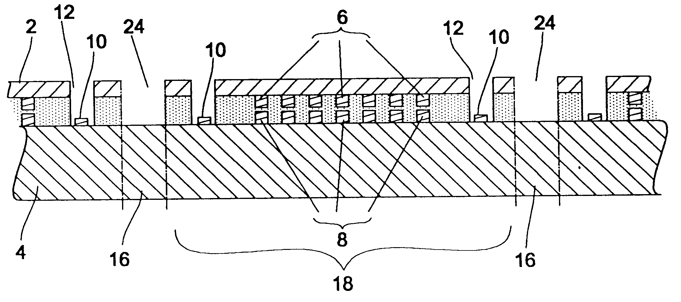
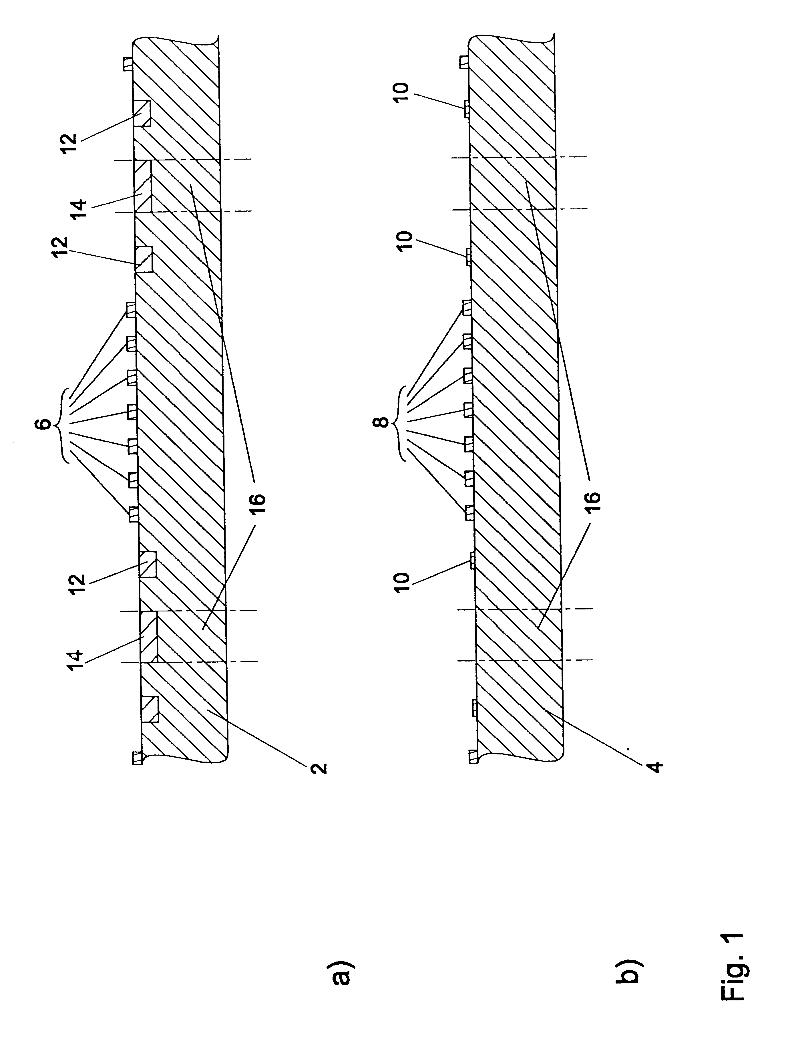
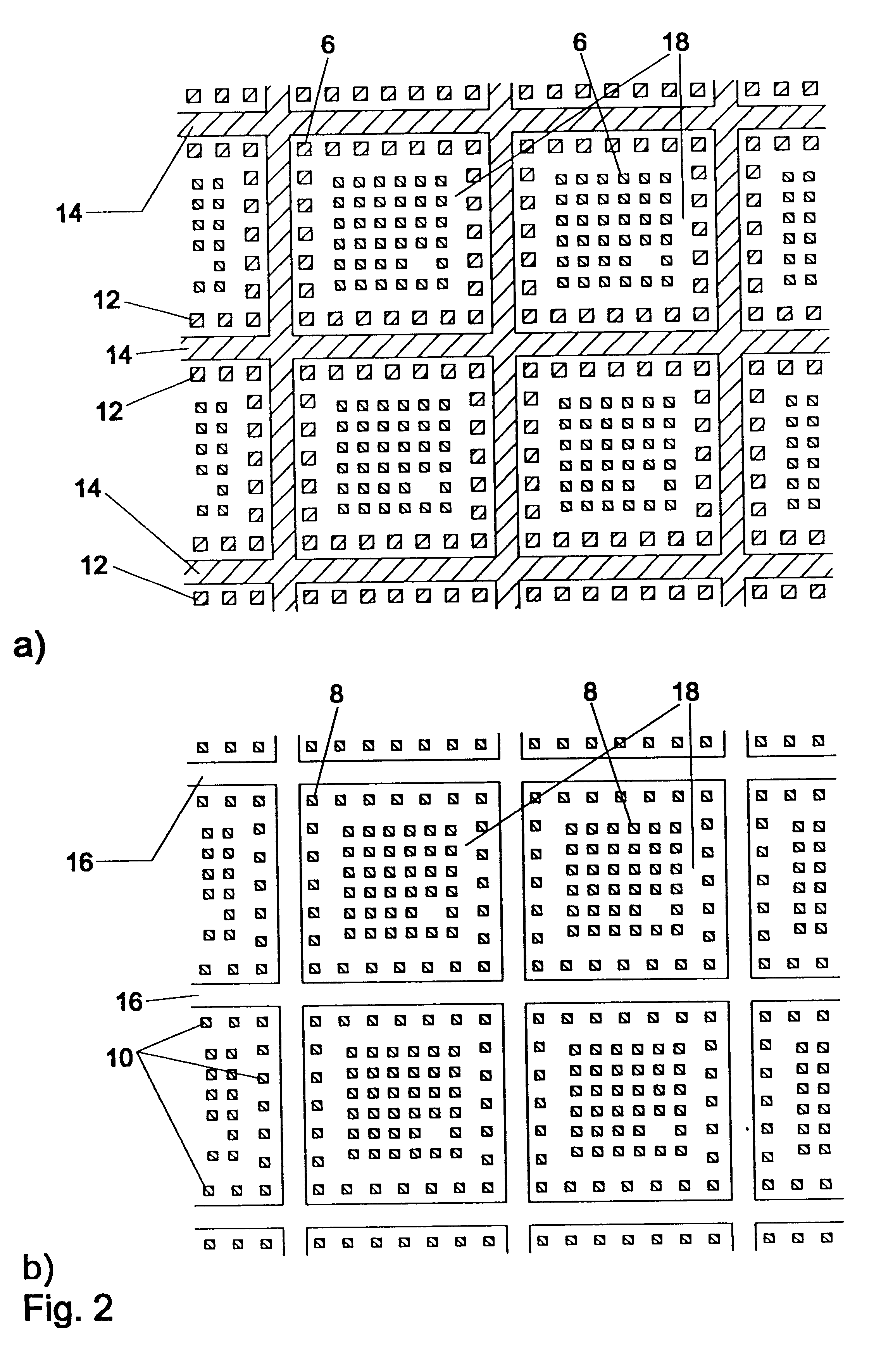
According to preferred embodiments of the present invention, two wafers are produced by identical or different standard production methods. In FIGS. 1a) and 1b) schematic cross-sectional views of two such wafers are shown, the wafer 2 shown in FIG. 1a) being referred to as upper wafer in the following, whereas the wafer 4 shown in FIG. 1b) will be referred to as lower wafer in the following.

The upper wafer 2 is provided with a plurality of connecting areas 6 which will be referred to as inner connecting areas in the following, since they are intended to be used for establishing a direct connection to inner connecting areas 8 of the lower wafer 4. The respective connecting areas 6 and 8 are arranged above integrated circuits (not shown) formed in the wafers 2 and 4. The integrated circuits are so to speak located in the upper main surfaces of the two wafers, i.e. for example in a thickness range of less than 2 .mu.m below the upper main surface. The lower wafer 4 is additionally prov...


PUM


Abstract

In a method for vertically integrating active circuit planes, a first substrate having at least one integrated circuit in a first main surface thereof and further having connecting areas for the integrated circuit as well as outer connecting areas on the first main surface is provided in a first step. A second substrate having at least one integrated circuit in a first main surface thereof and further having connecting areas for the integrated circuit as well as open or openable areas on the first main surface is provided. The first main surfaces of the first and second substrates are joined in such a way that the connecting areas of the first substrate are connected to those of the second substrate in an electrically conductive manner in such a way that the outer connecting areas of the first substrate are in alignment with the open or openable areas of the second substrate. Subsequently, the second substrate is thinned and the outer connecting areas are exposed through the open or openable areas. The resultant chips can be further processed making use of standard methods.

Description

1. Field of the InventionThe present invention relates to a method for vertically integrating two active circuit planes. In addition, the present invention relates to vertically integrated circuits produced by means of such methods.2. Description of Prior ArtIntegrated circuits arranged in a substrate are located essentially in the vicinity of a main surface of the substrate. In integrated circuits the active life of the transistors takes place only in the uppermost plane of the substrate, e.g. of the silicon crystal, in a thickness range of less than 2 .mu.m. The residual, a few hundred microns thick silicon of the substrate is not required for the circuit function. Hence, increasing efforts have been made for some time to utilize the third dimension, i.e. the thickness dimension more effectively.The production of an integrated circuit e.g. in CMOS technology normally comprises far more than 100 individual process steps; each of these process steps must be mastered separately with ...

Claims


Application Information

Patent Timeline
IPC IPC(8): H01L21/70H01L25/065H01L21/98
CPCH01L24/94H01L25/0657H01L25/50H01L2924/07802H01L2924/07811H01L2924/01068H01L2224/16145H01L2225/06513H01L2225/06517H01L2225/06541H01L2225/06593H01L2924/01013H01L2924/01015H01L2924/0102H01L2924/01057H01L2924/01058H01L2924/01061H01L2924/01082H01L2924/14H01L2924/01006H01L2924/01023H01L2924/01033H01L2924/00
Inventor FEIL, MICHAELLANDESBERGER, CHRISTOF
Owner S AQUA SEMICONDUCTOR LLC
Why Eureka
Try Eureka