Mechanism for enabling compliance with the IEEE standard 1149.1 for boundary-scan designs and tests

a boundary scan and design technology, applied in the field of integrated circuit testing (ics), can solve the problems of insufficient access to the desired hard macros, insufficient time for hard macros, and inability to achieve the desired propagation delay in the functional signal path

Inactive Publication Date: 2002-09-03
CISCO TECH INC
View PDF16 Cites 58 Cited by
  • Summary
  • Abstract
  • Description
  • Claims
  • Application Information

AI Technical Summary

Problems solved by technology

Objectionably, multiplexer 109 in scan cell 100 (FIG. 1) causes undesirable propagation delay in the functional signal path, especially in high-speed (above 200 Mhz clock) or timing-critical Application-Specific Integrated Circuit (ASIC) devices.
However, ASIC designers in many cases do not have access to the desired hard macros, and creating these hard macros requires additional time, resources, and in-depth knowledge of a device technology.
However, this software synthesis approach adds routing delay between "soft macro" components, introduces, in the boundary-scan cells, longer overall delay than the "hard macro" approach, and causes additional delay in the critical signal path, thereby encountering the same problem that is supposed to be solved.
Consequently, this software approach is unacceptable for high-speed designs.
Additionally, meeting the requirements of the boundary-scan standard in timing-critical and high-speed ASIC designs may be impractical because design time, resources, and device performance overhead costs are too high.
However, this solution leaves "holes" or incomplete pin fault coverage for a Device Under Test (DUT).
In cases where there is a need to test the uncovered pins, it is often impossible to add non-boundary scan-based test vectors to test those pins.
However, modification or design of custom test vectors requires additional ATE test generation and conversion time.

Method used


Image

  • Mechanism for enabling compliance with the IEEE standard 1149.1 for boundary-scan designs and tests
  • Mechanism for enabling compliance with the IEEE standard 1149.1 for boundary-scan designs and tests
  • Mechanism for enabling compliance with the IEEE standard 1149.1 for boundary-scan designs and tests

Examples


Embodiment Construction

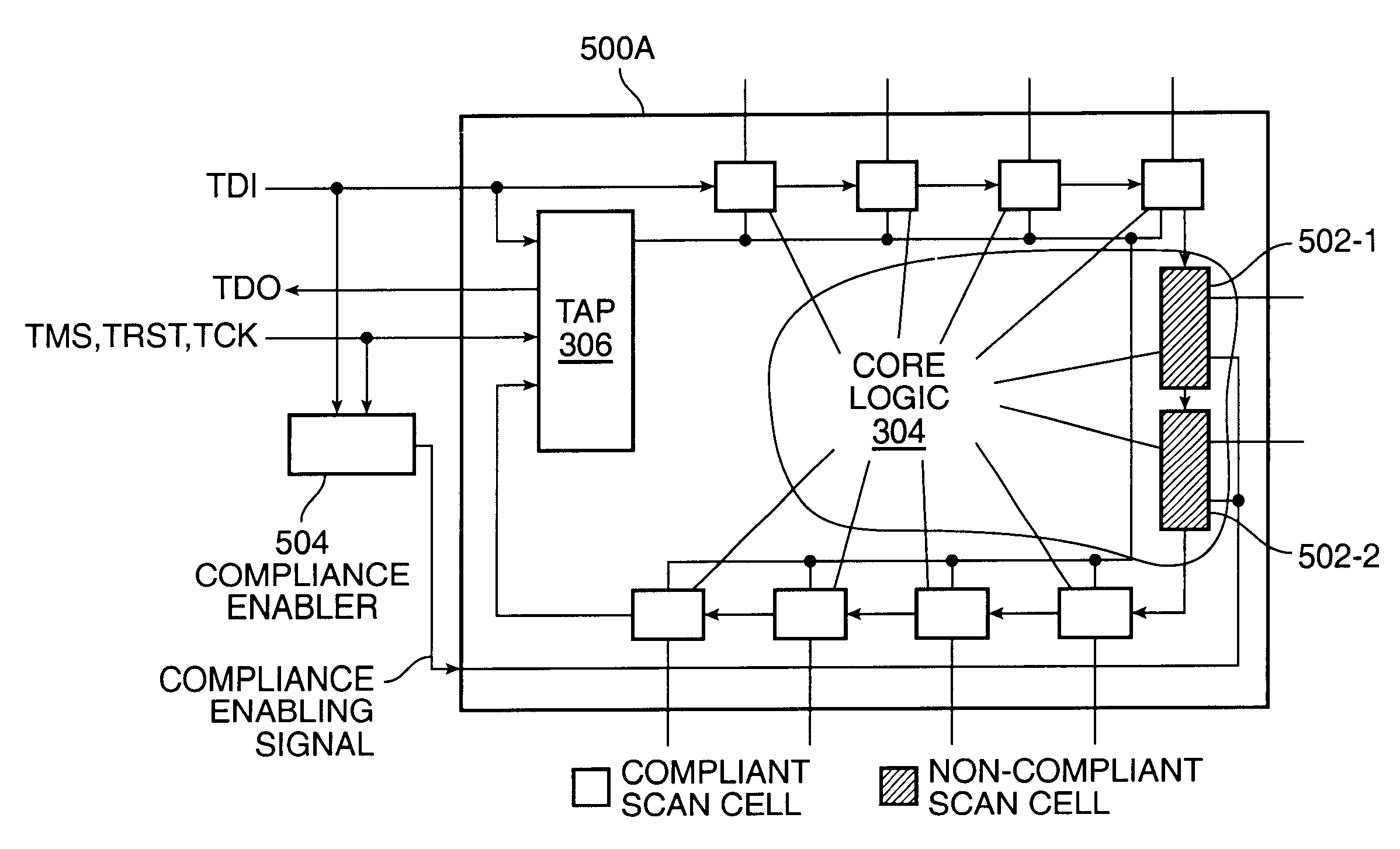
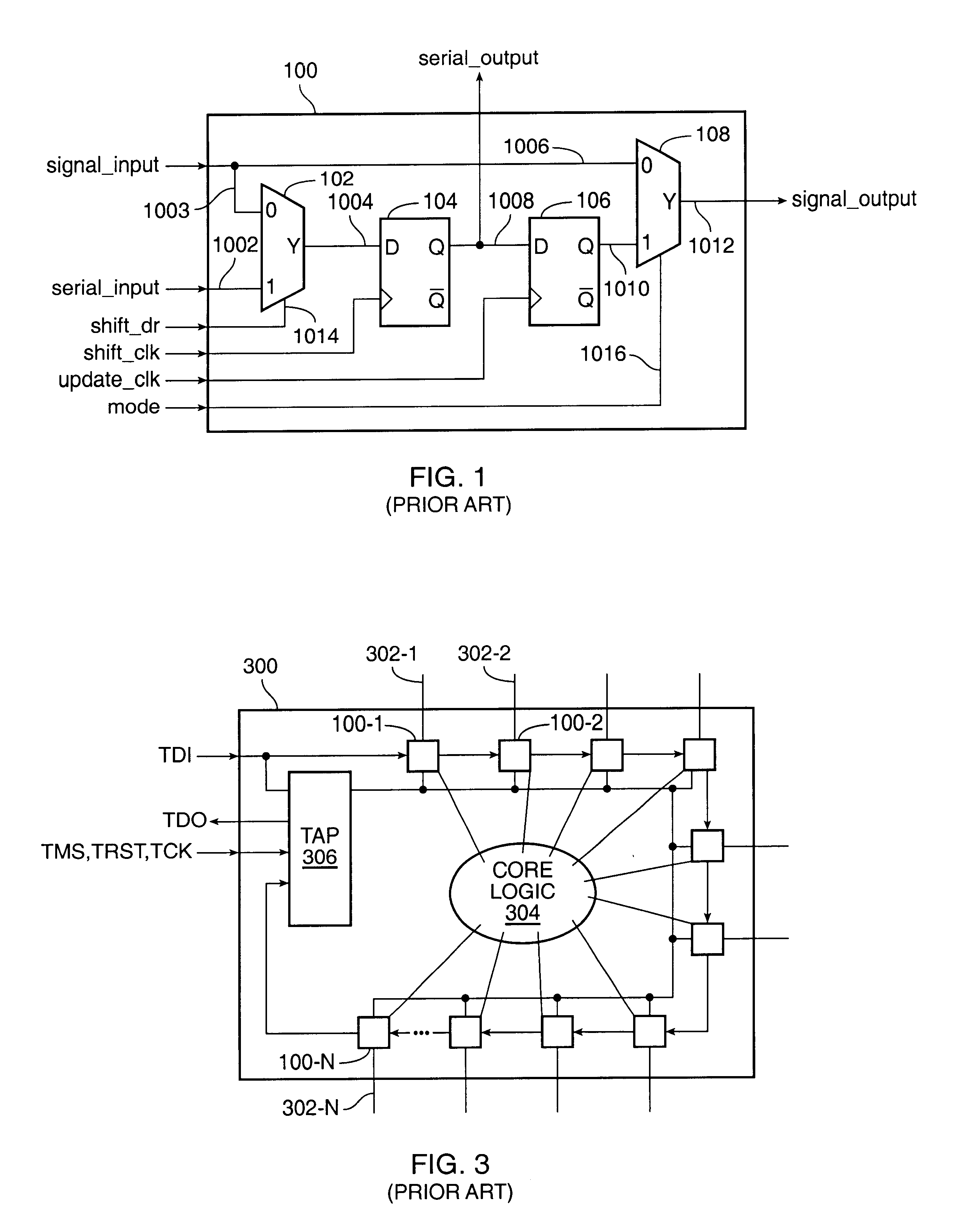
The present invention, in a first preferred embodiment, allows designing components with a non-compliant embedded boundary-scan cell structure while meeting all requirements of the IEEE standard 1149.1. In a second preferred embodiment the invention allows testing of devices that, due to size limitations for example, do not include an IEEE standard 1149.1 TAP controller. The invention thus enables test engineers to generate test vectors using existing both hardware and software tools that comply with the IEEE standard 1149.1. The invention also minimizes signal delay and gate overhead, permits meeting ASIC manufacturing test requirements, and improves IC testability, ASIC performance, ICT development time, and tester correlation and program reliability. LSSD- based scan cells can also use the invention.

FIG. 5A illustrates the invention in a first preferred embodiment as chip 500A, which is similar to FIG. 3 prior art chip 300 except that chip 500A includes two non-compliant scan cel...


PUM


Abstract

A mechanism for enabling compliance with the IEEE boundary-scan standard 1149.1 includes, in a first preferred embodiment, a compliance enabler working with non-compliant embedded boundary-scan cells to enable a Device Under Test (DUT) to function as an IEEE-standard-compliant part, thus allowing full utilization of existing test tool generation and operation of the IEEE standard. The enabler is preferably provided separately from boundary scan-cells embedded in core logic designs. The enabler includes a Test Access Port (TAP) controller and related decoding circuits to generate necessary compliance signals based on various conventional TAP controller variables and instruction functions. The embedded boundary-scan cells preferably include an internal scan cell architecture. In a second embodiment, a second enabler works with a TAP emulator to allow testing of TAP-less DUTs.

Description

1. Technical FieldThis invention relates generally to testing integrated circuits (ICs), and more particularly to testing according to the Institute of Electrical and Electronics Engineers (IEEE) standard 1149.1.2. Discussion of Background ArtTesting of integrated circuit devices or components is facilitated by providing each input and output (I / O) pin of the devices with a boundary-scan cell which enables using boundary-scan techniques to control and observe signals at the device boundaries. The IEEE standard 1149.1 specifies a boundary-scan architecture and a protocol which defines test logic that can be used with ICs in a standardized approach to testing the IC and interconnections between IC components when assembled on a printed circuit board or other substrate to form a product. The IEEE standard 1149.1 also allows observing or modifying circuit activity during otherwise normal operation of the circuit. Additionally, the defined test logic can access other design-for-test feat...

Claims


Application Information

Patent Timeline
Patent Type & Authority Patents(United States)
IPC IPC(8): G01R31/28G01R31/3185
CPCG01R31/318555G01R31/318572G01R31/318544
Inventor CHUNG, SUNG SOO
Owner CISCO TECH INC
Why Eureka
Try Eureka