
Family of analog amplifier and comparator circuits with body voltage control

a technology which is applied in the field of analog amplifier and comparator circuit with body voltage control, can solve the problems of body voltage flotation seriously erodes transistor matching, soi technology appears to be a poor choice for analog circuit,

Inactive Publication Date: 2002-09-17
IBM CORP
View PDF4 Cites 22 Cited by
  • Summary
  • Abstract
  • Description
  • Claims
  • Application Information

AI Technical Summary

Problems solved by technology

SOI technology would appear to be a poor choice for analog circuits.
Allowing the body voltage to float seriously erodes transistor matching.

Method used


Image

  • Family of analog amplifier and comparator circuits with body voltage control
  • Family of analog amplifier and comparator circuits with body voltage control
  • Family of analog amplifier and comparator circuits with body voltage control

Examples


Embodiment Construction

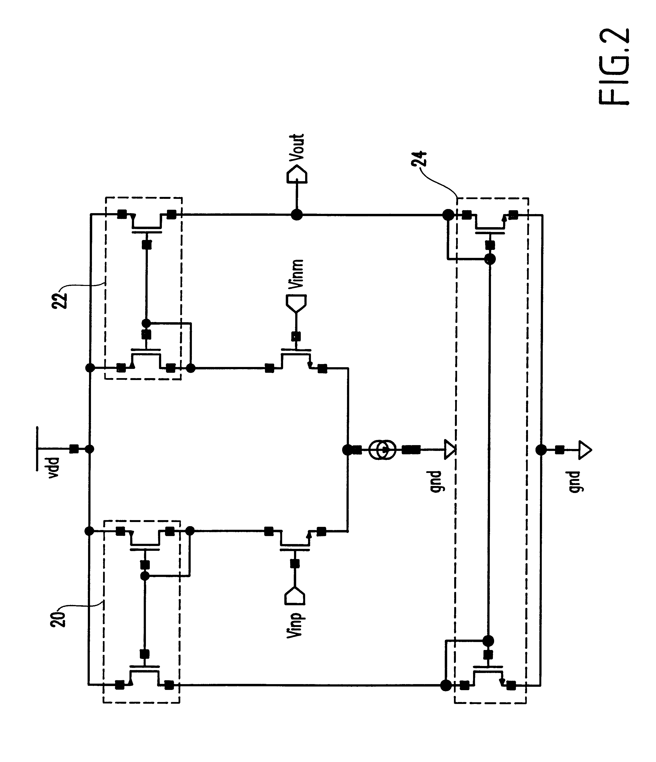
The invention will be explained, in a step by step fashion, from another well known amplifier commonly configured in bulk (non-SOI) technology.

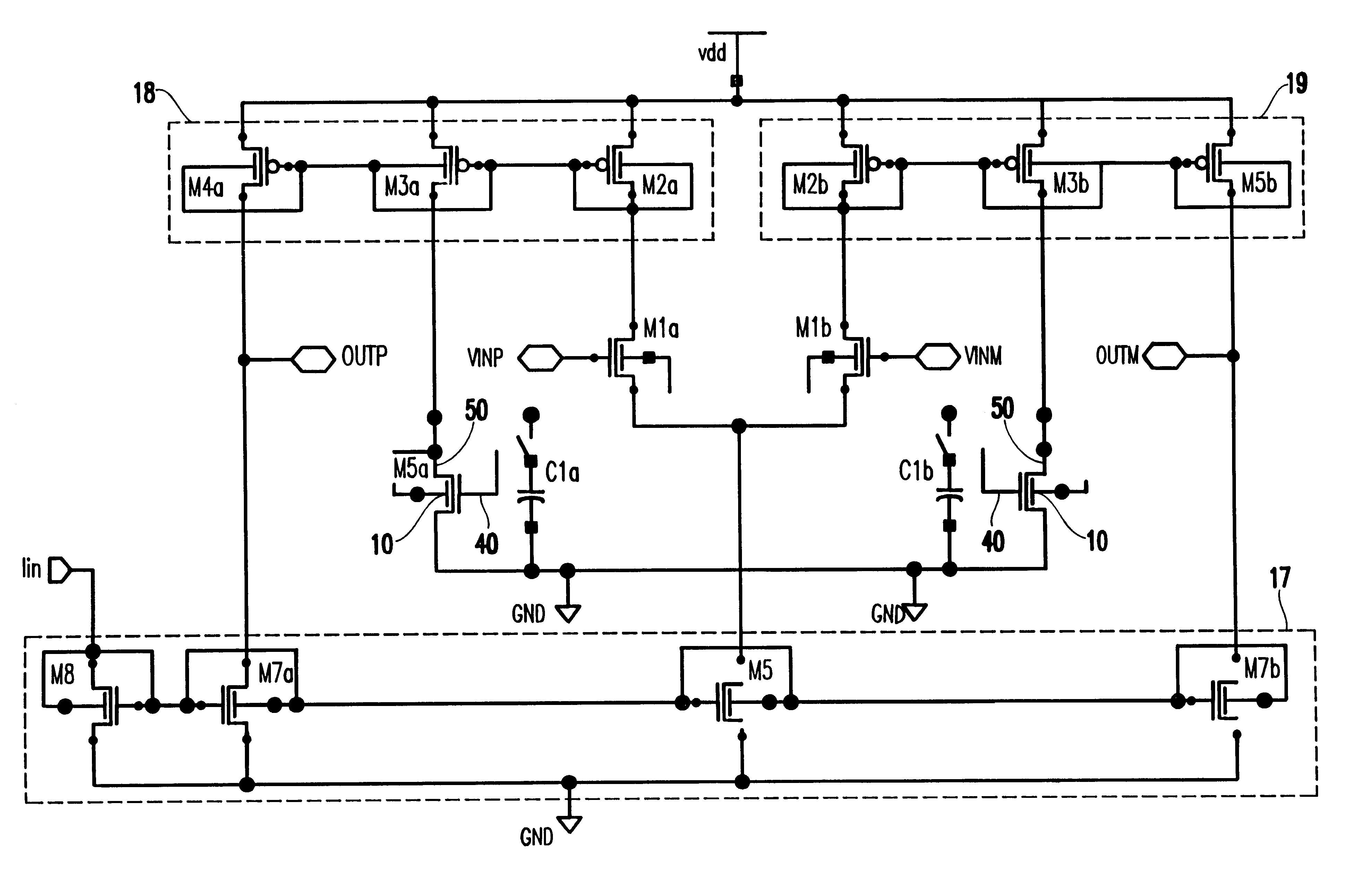
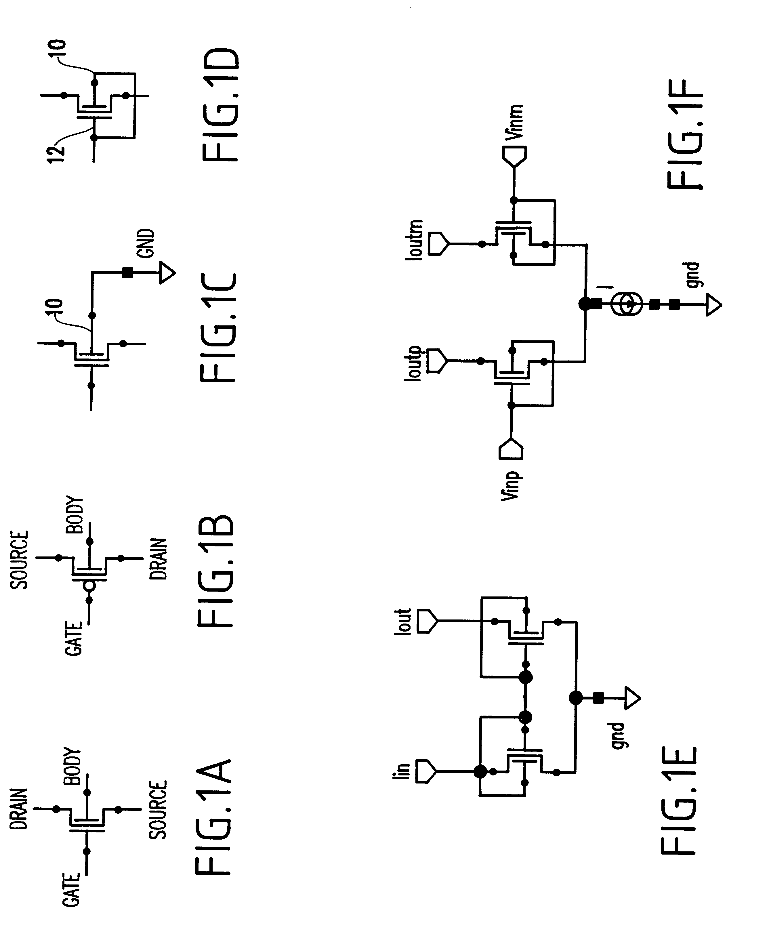
FIGS. 1a and 1b are schematic diagrams of n-channel and p-channel SOI FETs. SOI transistors are self contained within a pocket of insulating walls, and therefore, the SOI transistors have a body which is not joined to the substrate. This body can be treated like an independent electrode, or it can be externally wired to any of the other three electrodes (e.g., the body electrode could be wired to ground as in FIG. 1c). In this configuration, the SOI transistor behaves very much like a bulk transistor in a common substrate, and does not exhibit the "kink" effect or any other floating body effects so troublesome to conventional SOI analog circuits. However, it also doesn't exhibit any performance improvement. Thus, the price of SOI technology is paid without achieving any advantage.

FIG. 1d shows the body electrode 10 connected to the gate elect...


PUM


Abstract

A structure for an amplifier circuit which includes a pair of source-coupled differential transistors, each of source-coupled differential transistors having a body and a gate, and input transistors electrically connected to the source-coupled transistors. Also, the input transistors load the body and the gate of the source-coupled transistors with positive feedback signals. As a result, a differential gain is increased and a common mode gain is not increased. The output of the pair of source-coupled differential transistors is directed to second pair of transistors. The second pair of transistors generates mirrored voltages which track with input voltages. The second pair of transistors generates mirrored voltages translated by an offset voltage to values near ground, mirrored voltages which represent a voltage gain over an input voltage, and mirrored voltages which are largely differential and includes approximately no common mode input voltage.

Description

1. Field of the InventionThe present invention relates to amplifier circuits and more particularly to analog amplifier and comparator circuits with body voltage control.2. Description of the Related ArtSilicon On Insulator (SOI) technology offers performance enhancements over bulk silicon technology for Complimentary Metal Oxide Semiconductor (CMOS) digital circuits. When properly designed, circuits implemented in SOI should exhibit a 20% to 30% performance advantage over the same circuit functions implemented in bulk silicon. Alternately, the performance can be exchanged for a factor of two reduction in power dissipation at the same operating frequency. Much of this performance gain is achieved by letting the body voltage float. This arrangement allows the body voltage to bootstrap during switching transients resulting in more rapid "turn on" characteristic in the switching transistors. SOI technology has been projected to cost about 10% more than bulk technology.SOI technology wou...

Claims


Application Information

Patent Timeline
Patent Type & Authority Patents(United States)
IPC IPC(8): H03F3/45
CPCH03F3/4521H03F3/45748H03F2203/45342H03F2203/45658H03F2203/45711
Inventor BONACCIO, ANTHONY R.MICHAIL, MICHEL S.PRICER, WILBUR D.TANGHE, STEVEN J.
Owner IBM CORP
Learn More