Resin sealed semiconductor device utilizing a clad material heat sink

a technology of heat sink and resin sealing, which is applied in semiconductor devices, semiconductor/solid-state device details, cooling/ventilation/heating modification, etc., can solve the problems of thermal peeling and single metal material cannot meet all the three conditions at a satisfactory level

Inactive Publication Date: 2002-10-22
CITIZEN WATCH CO LTD
View PDF16 Cites 25 Cited by
  • Summary
  • Abstract
  • Description
  • Claims
  • Application Information

AI Technical Summary

Benefits of technology

Therefore, there can be obtained the metallic heat radiation member, which can satisfy three conditions required for the heat radiation member at a satisfactory level, i.e., (1) heat conductivity being excellent, (2) the difference of the coefficient of linear expansion between the heat radiation member and the sealing resin being small, and (3) adhesive properties to the sealing resin being good.
Furthermore, in the present invention, since the heat radiation member is constituted as the clad material, the heat radiation member having arbitrary properties can be obtained without increasing a processing cost.

Problems solved by technology

That is, in the case that the difference of the coefficient of linear expansion between the injection molded resin and the heat radiation member is excessively large, and when the IC chip generates heat, a warp force is generated between the resin and the member, so that thermal peeling occurs sometimes between the sealing resin and the heat radiation member.
However, any single metal material cannot satisfy all the three conditions at a satisfactory level.

Method used


Image

  • Resin sealed semiconductor device utilizing a clad material heat sink
  • Resin sealed semiconductor device utilizing a clad material heat sink
  • Resin sealed semiconductor device utilizing a clad material heat sink

Examples


first embodiment

[First Embodiment]

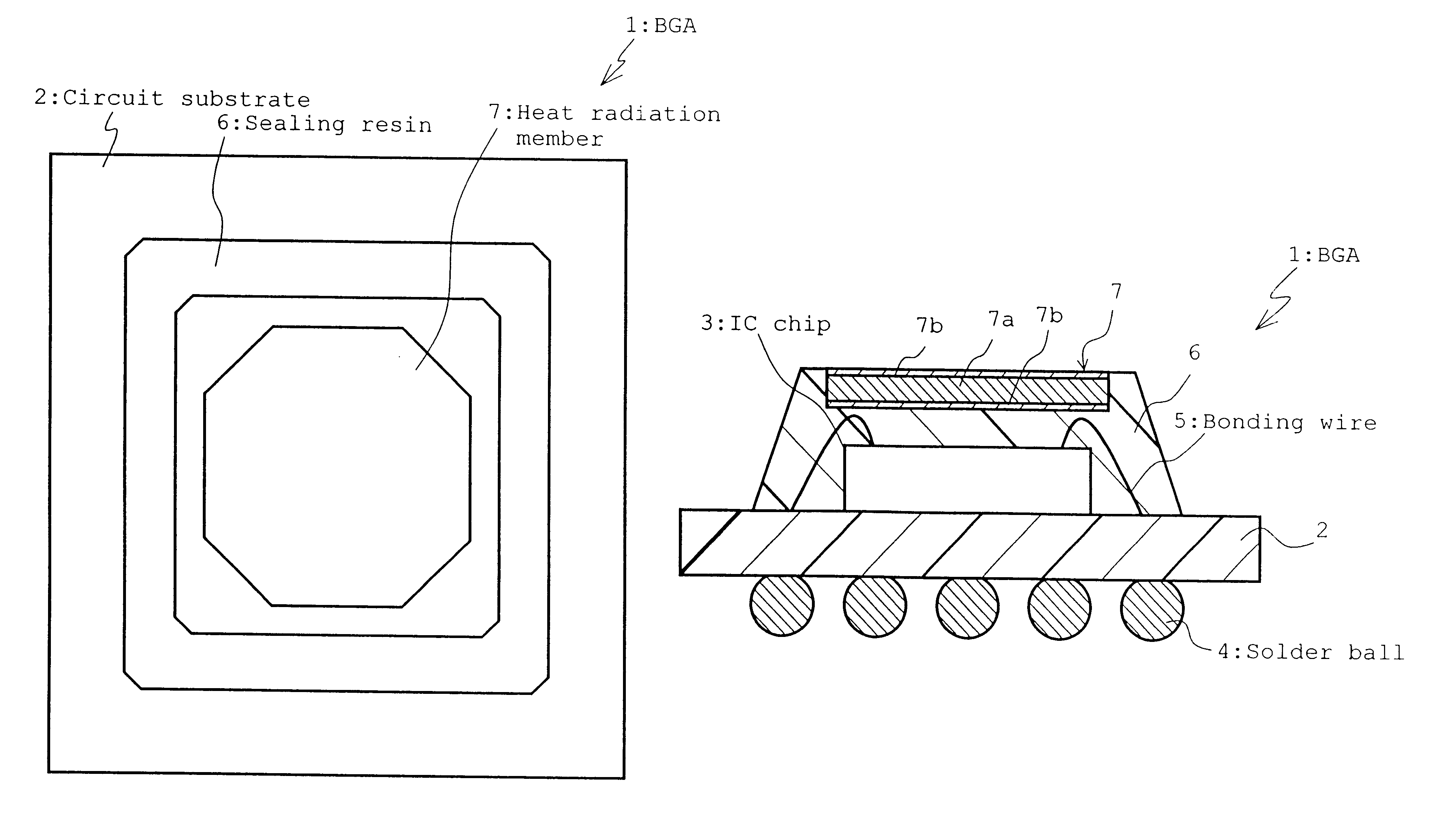
FIGS. 1A and 1B show a first embodiment of the present invention, wherein FIG. 1A is a plan view of a resin sealed ball grid array (hereinafter abbreviated as BGA), and FIG. 1B is a sectional view thereof.

As shown in the drawings, a BGA 1 is a semiconductor device comprising a resin circuit substrate 2, an IC chip 3, and solder balls 4 as contact electrodes, and the IC chip 3 is mounted on an upper surface of the circuit substrate 2, and is connected to upper-surface electrodes (not shown) of the circuit substrate 2 via bonding wires 5.

The upper-surface electrodes are connected to a plurality of solder balls 4 disposed on an underside of the substrate via through hole electrodes (not shown) formed on the circuit substrate 2.

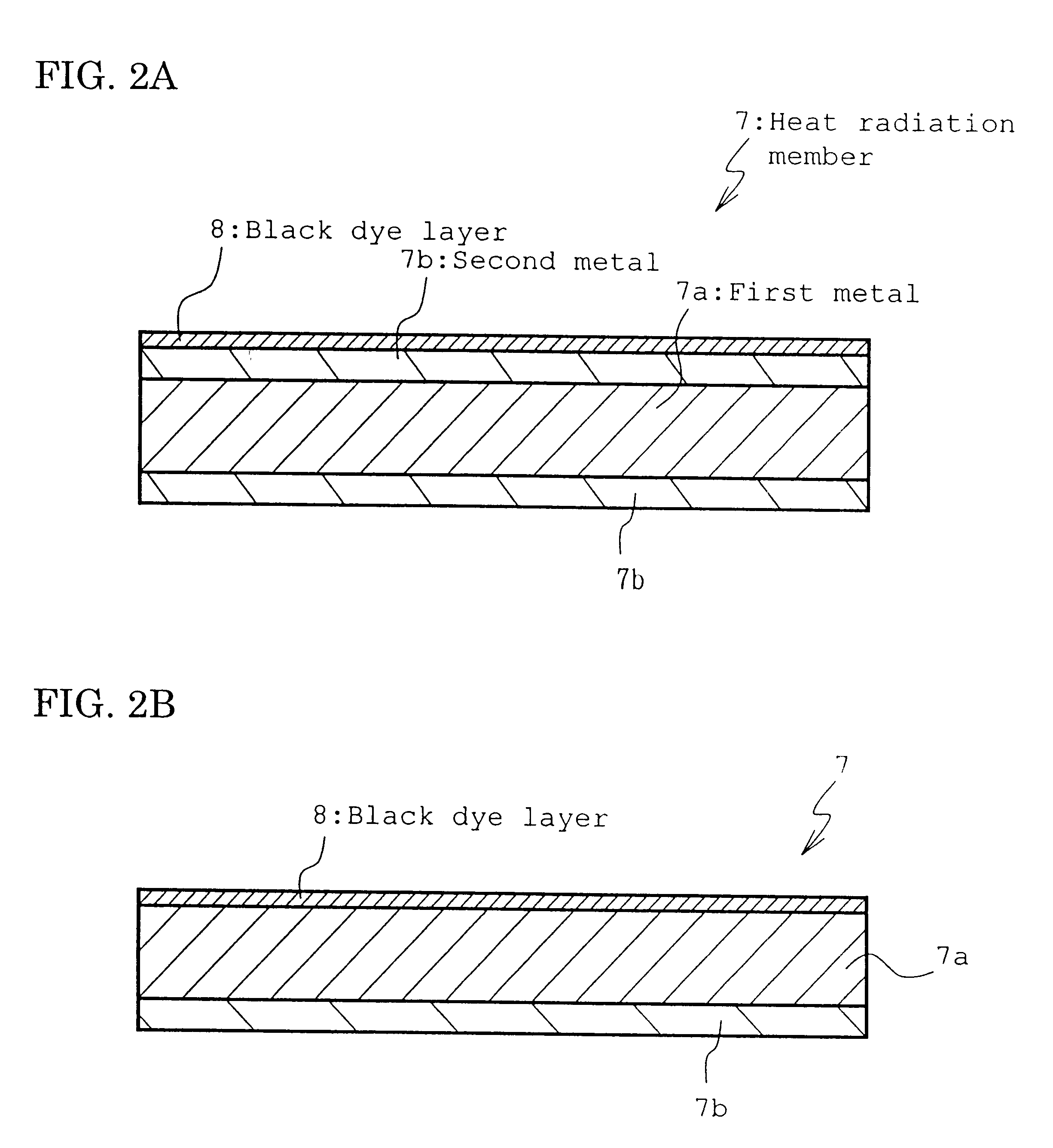
The IC chip 3 mounted on the circuit substrate 2 is resin-sealed by a sealing resin 6, and a metallic heat radiation member 7 is disposed above the IC chip 3. Then, the chip and the member are integrally fixed by the sealing resin 6.

Additionally...

second embodiment

[Second Embodiment]

FIGS. 3A and 3B show a second embodiment of the present invention, wherein FIG. 3A is a plan view of the BGA 1, and FIG. 3B is a sectional view thereof. In the drawings, parts similar to those of FIGS. 1A and 1B are denoted with the same reference numeral and detailed description thereof is omitted.

In the present embodiment shown in FIGS. 3A and 3B, similarly as first embodiment, a heat radiation member 17 is constituted of the clad material comprising the first metal 7a and the second metal 7b, and a protrusion 17a projecting on an IC chip 3 side is formed in a middle portion of the heat radiation member 17.

Since the protrusion 17a is formed on the heat radiation member 17, as shown in FIG. 3B, a distance between the IC chip 3 and the heat radiation member 17 can be reduced, the heat generated by the IC chip 3 can easily be conducted to the heat radiation member 17, and a heat radiation effect can further be enhanced.

Moreover, since the protrusion 17a projects on...

third embodiment

[Third Embodiment]

FIGS. 4A and 4B show a third embodiment of the present invention, wherein FIG. 4A is a sectional view of the BGA 1, and FIG. 4B is a perspective view of the heat radiation member. Incidentally, also in the drawings, the parts similar to those of FIGS. 1A and 1B are denoted with the same reference numerals and the detailed description thereof is omitted.

In the embodiment shown in FIGS. 4A and 4B, a through hole 27a projecting in a funnel shape on the IC chip 3 side is formed in the middle portion of a heat radiation member 27 comprising the first metal 7a and the second metal 7b.

In the embodiment shown in FIG. 4, a through hole 27a projecting in a funnel shape on the IC chip 3 side is formed in the middle portion of a heat radiation member 27 comprising the first metal 7a and the second metal 7b.

Since the through hole 27a is formed in the heat radiation member 27 in this manner, the resin can also be injected into the projecting through hole 27a during the injection...


PUM

PropertyMeasurementUnit
thicknessaaaaaaaaaa
thicknessaaaaaaaaaa
thicknessaaaaaaaaaa

Abstract

A resin sealed semiconductor device includes a heat radiation member fixed to a saling resin. The heat radiation member is formed of a clad material including a first metal having a coefficient of linear expansion close to that of the sealing resin, and a second metal laminated on the first metal and having good adhesive property to the sealing resin. Thus, the heat radiation member can satisfy all three conditions required for the heat radiation member at a satisfactory level, i.e., (1) heat conductivity being excellent, (2) a difference of a coefficient of linear expansion between the heat radiation member and a sealing resin being small, and (3) adhesive property to the sealing resin being good.

Description

1. Field of the InventionThe present invention relates to the improvement of a heat radiation structure of a resin sealed semiconductor device, and particularly, it relates to a heat radiation structure of a semiconductor device which can satisfy three conditions required for a heat radiation member, i.e., (1) heat conductivity being excellent, (2) a difference of a coefficient of linear expansion between the heat radiation member and a sealing resin being small, and (3) adhesive properties to the sealing resin being good.2. Description of the Related ArtA pin grid array (PGA) and a ball grid array (BGA) have generally been known as semiconductor devices in which high-density mounting is possible. Each of the PGA and BGA is a semiconductor device which is manufactured by mounting an IC chip on a resin substrate having a plurality of contact electrodes on an underside, and then sealing the IC chip on the substrate with a resin.Moreover, in recent years, this type of PGA and BGA has b...

Claims


Application Information

Patent Timeline
Patent Type & Authority Patents(United States)
IPC IPC(8): H01L23/433H01L23/34H01L23/28H01L21/56H01L23/12H01L23/373
CPCH01L23/4334H01L2224/48227H01L2924/01079H01L2924/15311H01L2924/16152H01L2924/3025H01L24/48H01L2924/01019H01L2924/16251H01L2224/05599H01L2224/45099H01L2224/85399H01L2924/00014H01L2924/12042H01L2924/181H01L2924/1815H01L2924/00H01L2224/45015H01L2924/207
Inventor SORIMACHI, KAZUAKIKIKUCHI, MASAYOSHI
Owner CITIZEN WATCH CO LTD
Why Eureka
Try Eureka