Semiconductor device

a technology of semiconductor devices and semiconductors, applied in non-linear optics, instruments, optics, etc., can solve the problems of deteriorating phenomena, crystalline tft still inferior in reliability to mos transistors, and severe specifications for liquid crystal display devices

Inactive Publication Date: 2002-12-31
SEMICON ENERGY LAB CO LTD
View PDF36 Cites 485 Cited by
  • Summary
  • Abstract
  • Description
  • Claims
  • Application Information

AI Technical Summary

Problems solved by technology

Specifications required of the liquid crystal display device are severe.
In this regard, it is said that the crystalline TFT is still inferior in point of reliability to a MOS transistor (a transistor fabricated on a single-crystal semiconductor substrate) which is used for an LSI, etc.
A cause for the deteriorating phenomena is the injection of hot carriers, that is, the hot carriers created by a high electric field near the drain of the TFT incur the deteriorating phenomena.

Method used


Image

  • Semiconductor device
  • Semiconductor device
  • Semiconductor device

Examples


embodiment 1

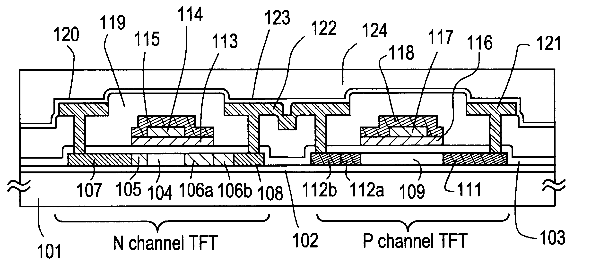
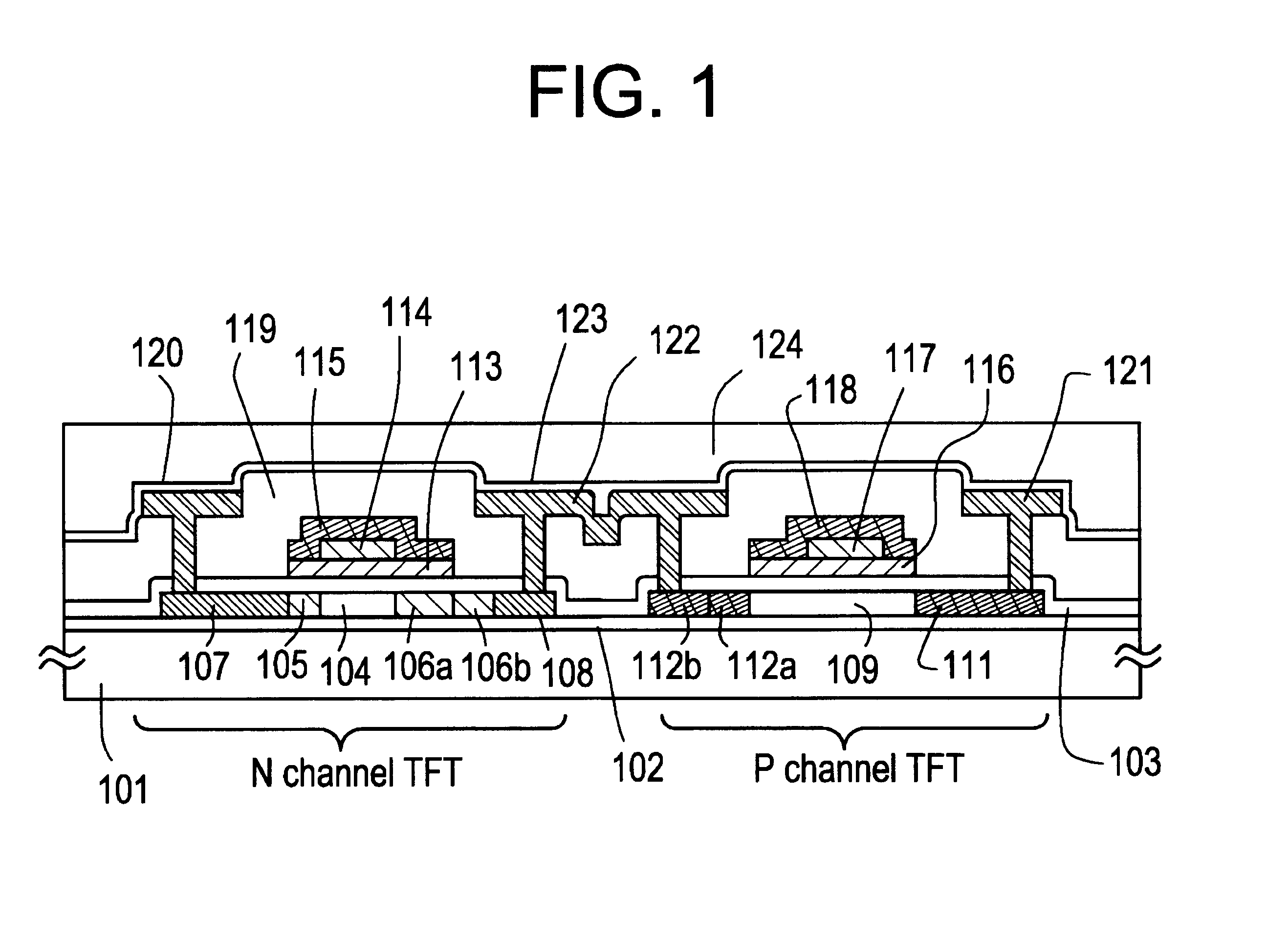
In this embodiment, the construction of the present invention will be described concerning a method in which a pixel matrix circuit, and a CMOS circuit being the basic form of a drive circuit to be provided around the pixel matrix circuit are fabricated simultaneously.

Referring to FIGS. 3A through 3C, a substrate 301 is a non-alkaline glass substrate which is typified by 1737 Glass Substrate of Corning Incorporated. An underlying film 302 is formed on that surface of the substrate 301 on which TFTs are to be formed, by plasma CVD or sputtering. Though not shown, a silicon nitride film being 25 to 100 nm, typically 50 nm thick, and a silicon oxide film being 50 to 300 nm, typically 150 nm thick, are formed as the underlying film 302.

Alternatively, the underlying film 302 may be formed by stacking a silicon oxide nitride film which is produced from SiH.sub.4, NH.sub.3 and N.sub.2 O by plasma CVD to a thickness of 10 to 200 nm (preferably 50 to 100 nm), and a silicon oxide nitride film...

embodiment 2

In this embodiment, there will be described another aspect of performance in which a pixel matrix circuit, and a CMOS circuit being the basic form of a drive circuit to be provided around the pixel matrix circuit are fabricated simultaneously in the same manner as in Embodiment 1.

First, as in Embodiment 1, the steps of FIGS. 3A through 3C and FIG. 4A are carried out.

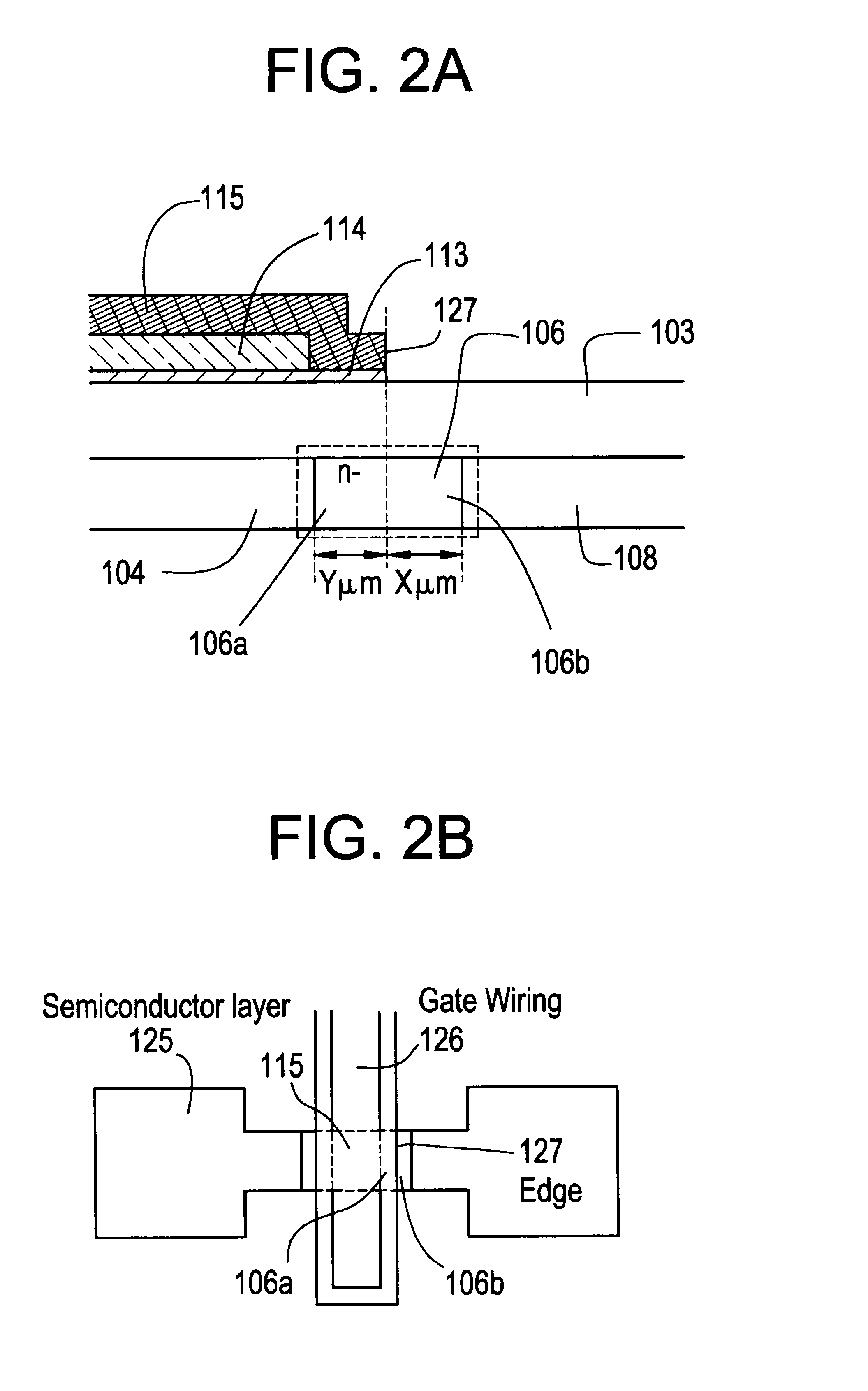
FIG. 6A illustrates the state in which each of the gate electrodes is formed of the first layer, the second layer and the third layer. The substrate in this state is formed with resist masks 601, 602, 603, 604, 605, and is subjected to the step of doping with an impurity element which bestows the n-conductivity type. Thus, first impurity regions 606, 607, 608, 609, 610, 611, 612 are formed (FIG. 6B).

Each of the resist masks 601, 602 formed here is in a shape in which an LDD region is formed on only the side of the drain region of the TFT. In other words, that part of the resist mask which masks a second impurity region f...

embodiment 3

In this embodiment, there will be described another aspect of performance in which a pixel matrix circuit, and a CMOS circuit being the basic form of a drive circuit to be provided around the pixel matrix circuit are fabricated simultaneously in the same manner as in Embodiment 1.

First, as in Embodiment 1, the steps of FIGS. 3A through 3C are carried out.

At the next step as illustrated in FIG. 8A, using a known patterning technique, resist masks 801, 802, 803, 804, 805 are formed, and the conductive layer (C) 321 and the conductive layer (A) 307 are partly removed. Here, the step of the removal is implemented by dry etching as in Embodiment 1. Thus, the first layers 851, 852, 853, 854, 855 of respective gate electrodes and the third layers 856, 857, 858, 859, 860 thereof are formed. The lengths of the first layer of each gate electrode and the third layer thereof in the channel length direction are set equal. The first layers 851, 852 of the gate electrodes of the CMOS circuit and t...


PUM

PropertyMeasurementUnit
gate voltageaaaaaaaaaa
thickaaaaaaaaaa
thickaaaaaaaaaa

Abstract

The gate electrode of a crystalline TFT is constructed as a clad structure which consists of a first gate electrode, a second gate electrode and a third gate electrode, thereby to enhance the thermal resistance of the gate electrode. Besides, an n-channel TFT is provided with a low-concentration impurity region which adjoins a channel forming region, and which includes a subregion overlapped by the gate electrode and a subregion not overlapped by the gate electrode, thereby to mitigate a high electric field near the drain of the TFT and to simultaneously prevent the OFF current of the TFT from increasing.

Description

1. Field of the InventionThe present invention relates to a semiconductor device in which a circuit including a thin film transistor (hereinbelow, abbreviated to "TFT") is formed on a substrate having an electrically insulating surface, and a method of fabricating the semiconductor device. By way of example, it relates to the constructions of an electrooptic device which is typified by a liquid crystal display device, and an electronic equipment in which the electrooptic device is installed. Incidentally, here in this specification, the expression semiconductor device is intended to signify general devices which function by utilizing semiconductor properties, and it shall cover within its category such electrooptic device and the electronic equipment as exemplified above.2. Description of the Related ArtThere have been positively fostered the developments of techniques for fabricating an active matrix type liquid crystal display device by providing TFTs on a glass substrate or a qua...

Claims


Application Information

Patent Timeline
Patent Type & Authority Patents(United States)
IPC IPC(8): G02F1/13G02F1/1368H01L21/28H01L29/66H01L21/336H01L27/12H01L29/786H01L21/02H01L29/40H01L29/49H01L21/70H01L29/423H01L21/84H01L21/77
CPCG02F1/1368H01L21/28114H01L29/42384H01L29/4908H01L29/66757H01L29/78627H01L27/088H01L29/786H01L27/124H01L29/78624H01L2029/7863
Inventor YAMAZAKI, SHUNPEI
Owner SEMICON ENERGY LAB CO LTD
Why Eureka
Try Eureka