Output controlled line driver with programmable common mode control

a technology of output control and common mode control, applied in logic circuit coupling/interface arrangement, pulse technique, baseband system details, etc., can solve the problems of unterminated circuit portions composed of package parasitics and internal circuitry, add additional system costs for off-chip components, and reduce the performance of the system, so as to achieve superior electrical source impedance termination and cost saving

Inactive Publication Date: 2003-01-07
INFINEON TECH AG
View PDF2 Cites 64 Cited by
  • Summary
  • Abstract
  • Description
  • Claims
  • Application Information

AI Technical Summary

Benefits of technology

Thus, the present invention has many advantages and benefits over the prior art. For example, the present invention may offer a cost savings by eliminating the need for external termination components. Additionally, the present invention may provide superior electrical source impedance termination of the transmit line driver. That is, the system and method of the present invention terminate the output of the line driver, creating a system which is insensitive to manufacturing process tolerances, temperature and supply variations. Moreover, since the present system and method terminate the driver inside the chip, at the output of the line driver, signal reflections on the signal line are kept to a minimum. Beneficially, post manufacturing calibration of the output voltage swing, output common mode voltage level, and output termination resistor value may be performed independently.

Problems solved by technology

Off-chip components add additional system costs and are generally outside the control of the chip fabricator which may result in system performance degradation.
Generally, off-chip termination results in unterminated circuit portions composed of package parasitics and internal circuitry.
These unterminated circuit portions can cause large reflections on the signal line.
Prior art devices and methods having integrated open drain output drivers, and internal fixed or external fixed termination resistors are limited, providing only fixed output voltage swing and fixed common mode voltage levels.
The voltage drop across these inductances causes problems at higher switching speeds.
Prior art systems and methods do not provide sufficient electrical control of the output driver's source impedance.
However, CMOS application processes do not provide a material from which accurate and temperature insensitive resistors may be produced.

Method used


Image

  • Output controlled line driver with programmable common mode control
  • Output controlled line driver with programmable common mode control
  • Output controlled line driver with programmable common mode control

Examples


Embodiment Construction

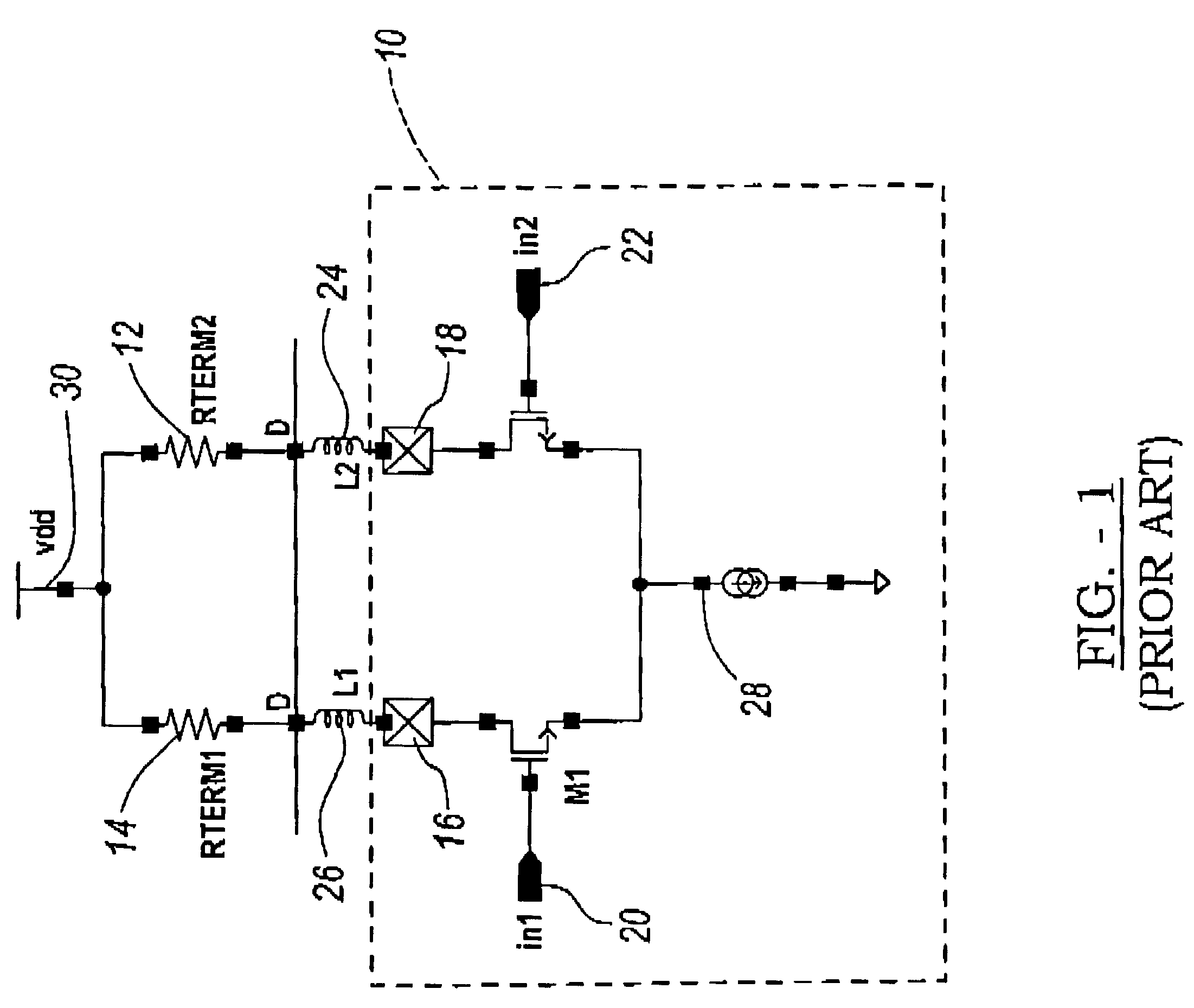
FIG. 1 illustrates a prior art system and method for terminating an integrated circuit (IC) 10. Typically, IC 10 is terminated using external termination resistors, such as resistors 12 and 14. IC 10 includes at least two bonding pads 16 and 18 for connecting, for example, input transistors 20 and 22 to external termination resistors 12, 14. In practice, bonding pads 16 and 18 are wire bonded to the external termination resistors 12 and 14 using wire bonds 24 and 26.

Input transistors 20 and 22 are connected to a negative supply voltage via the current source 28, and the external termination resistors 12 and 14 are connected to a positive power supply voltage 30. In this manner, chip termination may be achieved.

Typically, IC 10 is a differential open drain output driver having external termination resistors 12, 14. Such line drivers have limited versatility in that they provide only a fixed output voltage swing and fixed common mode levels. Moreover, the output current of the integra...


PUM


Abstract

A differential line driver having integrated output termination resistors is disclosed. The termination resistors are a combination of a controlled transistor and a low precision resistor. The transistor calibrates-out the imprecision of the resistor based on a precise electrical reference. In a preferred embodiment the transistor is a CMOS transistor and the resistor is a CMOS resistor. The combination of a CMOS transistor and CMOS resistor features higher linearity and precision than a CMOS transistor alone due to the smaller effective drain-source voltage across the CMOS transistor. Moreover, the present invention discloses independent programmability of the integrated output termination resistor, the output common mode voltage, and the output amplitude. The value of the output termination resistor(s), the value of the output common mode voltage, and the value of the output amplitude are controlled independently and are continuously maintained with respect to a precise electrical reference. As a result, the value of the output termination resistance, the value of the output common mode voltage, and the value of the output amplitude are insensitive to manufacturing process tolerances and variations in temperature and supply voltage.

Description

The present invention relates to CMOS signaling and transmit drivers and specifically to devices and methods for terminating such drivers.Typically, transmit drivers used in CMOS signaling applications utilize discreet off-chip resistors for output termination. Off-chip components add additional system costs and are generally outside the control of the chip fabricator which may result in system performance degradation. Generally, off-chip termination results in unterminated circuit portions composed of package parasitics and internal circuitry. These unterminated circuit portions can cause large reflections on the signal line.Prior art devices and methods having integrated open drain output drivers, and internal fixed or external fixed termination resistors are limited, providing only fixed output voltage swing and fixed common mode voltage levels. Moreover, the output current of the integrated open drain driver flows through a bond wire and package inductance to create a voltage si...

Claims


Application Information

Patent Timeline
Patent Type & Authority Patents(United States)
IPC IPC(8): H04L25/02H03K19/0175
CPCH04L25/0276H04L25/028H04L25/0278H03K17/16
Inventor HART, SIEGFRIEDSETTY, PALAKSHA
Owner INFINEON TECH AG
Why Eureka
Try Eureka