Method for wrapped-gate MOSFET

a technology of mosfet and wrap-gate, which is applied in the direction of semiconductor devices, electrical devices, transistors, etc., can solve the problems of new problems and challenges in the industry

Inactive Publication Date: 2003-01-21
IBM CORP
View PDF5 Cites 21 Cited by
  • Summary
  • Abstract
  • Description
  • Claims
  • Application Information

AI Technical Summary

Problems solved by technology

As device size shrinks, the industry has been observing new problems and challenge...

Method used


Image

  • Method for wrapped-gate MOSFET
  • Method for wrapped-gate MOSFET
  • Method for wrapped-gate MOSFET

Examples


Embodiment Construction

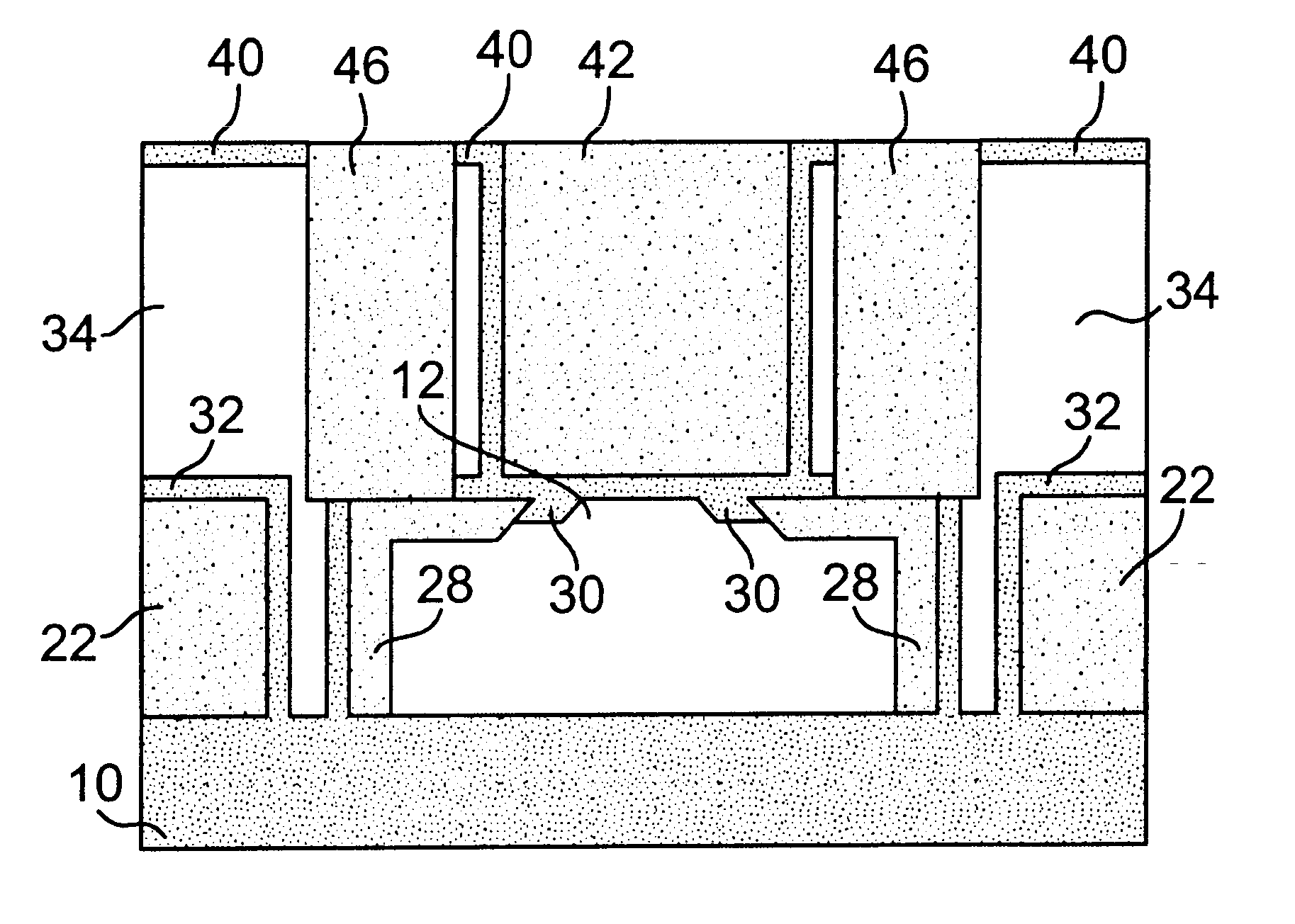
The present invention provides an improved gate control scheme by forming a wrapped gate electrode which surrounds a channel region from multiple dimensions.

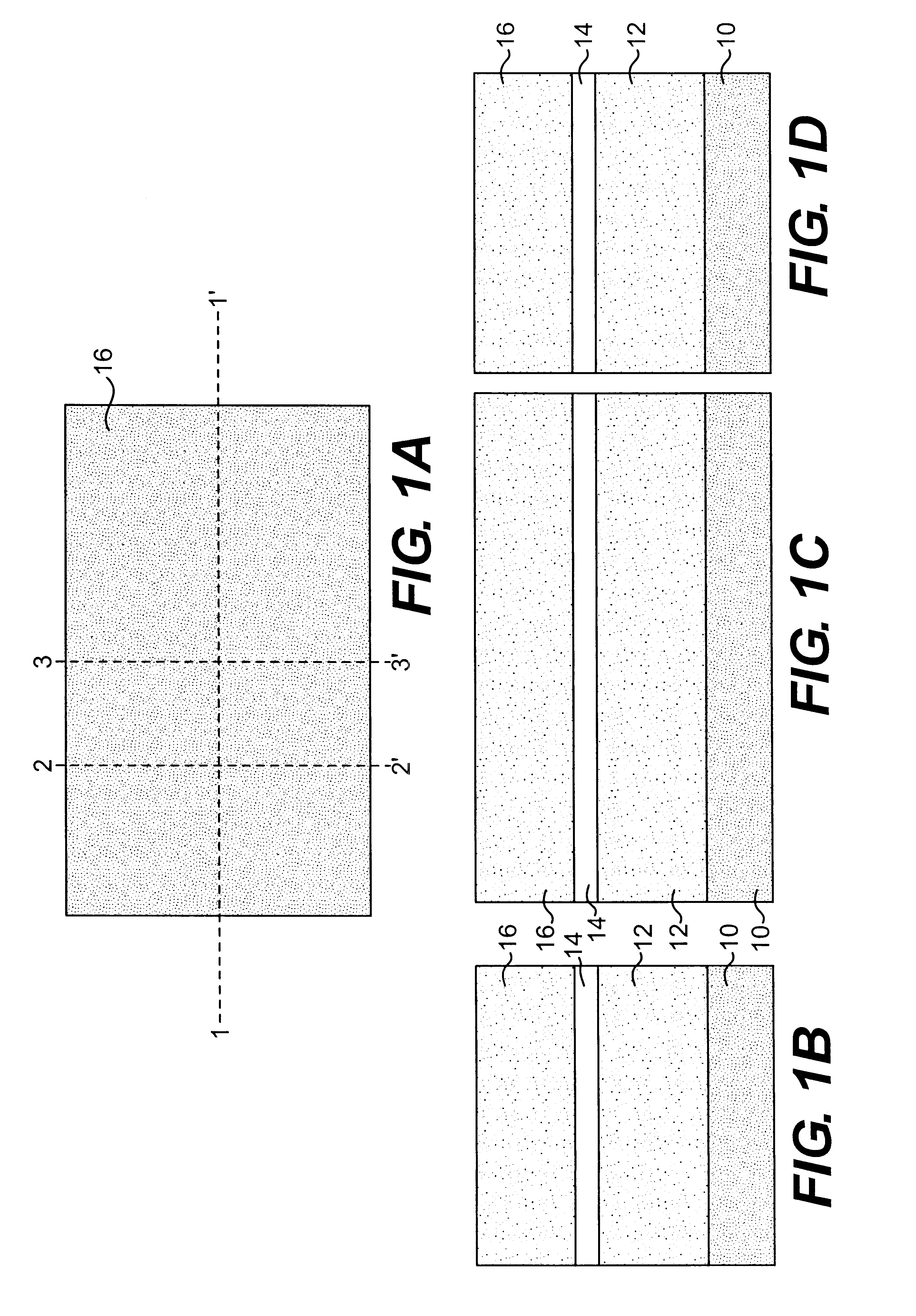
Referring now to the drawings, and more particularly to FIGS. 1A-1D, there is shown a structure formed based on an SOI substrate. The SOI substrate includes a buried insulation layer 10, a top silicon layer 12 formed on the buried insulation layer 10. A bottom silicon substrate on which the buried insulation layer 10 is formed is not shown. As shown in FIGS. 1B, 1C and 1D, the structure further includes a dummy gate oxide layer 14 formed on the top silicon layer 12 and a nitride pad layer 16 formed on the dummy gate oxide layer 14.

As shown in FIG. 1A which depicts the top view of the structure, the pad nitride layer 16 is entirely covering the structure. FIG. 1B depicts a cross-sectional view of the structure dissected by dotted line 2-2'. FIG. 1C depicts a cross-section view of the structure dissected by dotted line 1-1'. FIG. ...


PUM


Abstract

A wrapped-gate transistor includes a substrate having an upper surface and first and second side surfaces opposing to each other. Source and drain regions are formed in the substrate with a channel region therebetween. The channel region extends from the first side surface to the second side surfaces of the substrate. A gate dielectric layer is formed on the substrate. A gate electrode is formed on the gate dielectric layer to cover the channel region from the upper surface and the first and second side surfaces with the gate dielectric therebetween. The substrate is a silicon island formed on an insulation layer of an SOI (silicon-on-insulator) substrate or on a conventional non-SOI substrate, and has four side surfaces including the first and second side surfaces. The source and drain regions are formed on the portions of the substrate adjoining the third and fourth side surfaces which are perpendicular to the first and second side surfaces. The wrapped-gate structure provides a better and quicker potential control within the channel area, which yields steep sub-threshold slope and low sensitivity to the "body-to-source" voltage.

Description

DESCRIPTIONBackground of the Invention1. Field of the InventionThe present invention generally relates to the fabrication of metal oxide semiconductor field effect transistors (MOSFET) and, more particularly, to a MOSFET devices having a wrapped-gate structure.2. Background DescriptionThe escalating requirements for high performance and density associated with ultra large scale integration semiconductor devices require high speed and reliability and increased manufacturing throughput for competitiveness.Integrated circuits, including transistors, are typically formed from either bulk silicon starting material, silicon on insulator (SOI) starting material, or SOI material that is formed from a bulk semiconductor starting material during processing. A gate dielectric layer, typically an oxide, is formed on the starting material (i.e., substrate) and a gate electrode, typically polysilicon, is formed on the gate dielectric layer. Source and drain regions are formed in the substrate, ty...

Claims


Application Information

Patent Timeline
IPC IPC(8): H01L29/66H01L21/336H01L29/786H01L21/02H01L29/40H01L29/423H01L29/417H01L29/41H01L29/78
CPCH01L29/41733H01L29/42384H01L29/78618H01L29/66795H01L29/785H01L29/66545H01L21/18
Inventor PARK, BYEONGJUFURUKAWA, TOSHIHARUMANDELMAN, JACK A.
Owner IBM CORP
Why Eureka
Try Eureka