Unlock instant, AI-driven research and patent intelligence for your innovation.

Driving circuit for LCD

a driving circuit and circuit technology, applied in the direction of logic circuit coupling/interface arrangement, pulse technique, instruments, etc., can solve the problems of increasing the total power consumption and serious problems arising from the trend toward a larger screen

Inactive Publication Date: 2003-05-06
LAPIS SEMICON CO LTD
View PDF8 Cites 10 Cited by
  • Summary
  • Abstract
  • Description
  • Claims
  • Application Information

AI Technical Summary

Benefits of technology

Accordingly, it is an object of the present invention to provide a driving circuit in which the problems of the prior art are solved and in which no leakage current occurs in switching of a driving voltage.
According to a sixth aspect of the present invention, there is provided a driving circuit for outputting any one of a plurality of driving voltages to a common output node, the driving circuit including: a driving signal output circuit for outputting a plurality of driving signals corresponding to the plurality of driving voltages on the basis of a plurality of selection signals; and a plurality of switching units, which are controlled by the plurality of driving signals, respectively, for outputting the driving signal corresponding to any one of the plurality of driving voltages to the output node, wherein the driving signal output circuit is constructed so as to generate the plurality of driving signals to allow a transition from an ON state to an OFF state of the switching unit to be faster than that from the OFF state to the ON state thereof.
The driving signal to allow the transition from the ON state to the OFF state to be faster than that from the OFF state to the ON state is outputted from the driving signal output circuit to the switching unit. Consequently, a fear of simultaneously turning on the plurality of switching units is eliminated.
According to a seventh aspect of the present invention, there is provided a driving circuit for outputting one of first and second driving voltages to a common output node, the driving circuit including: a first driving signal output circuit for outputting a first driving signal corresponding to the first driving voltage on the basis of a first selection signal; a second driving signal output circuit for outputting a second driving signal corresponding to the second driving voltage on the basis of a second selection signal; a first switching unit, which is controlled by the first driving signal, for outputting the first driving voltage to the output node; and a second switching unit, which is controlled by the second driving signal, for outputting the second driving voltage to the output node, wherein the first and second driving signal output circuits output the first and second driving signals for allowing a transition from an ON state to an OFF state of the second switching unit to be faster than that from the OFF state to the ON state of the first switching unit, respectively.

Problems solved by technology

Although the leakage current caused in each driving circuit is small, as the number of driving circuits is increased in association with a trend toward a larger screen of the LCD, the total power consumption is increased.
The increase in power consumption associated with the trend toward the larger screen is a serious problem especially in battery-powered portable displays.

Method used


Image

  • Driving circuit for LCD
  • Driving circuit for LCD
  • Driving circuit for LCD

Examples


first embodiment

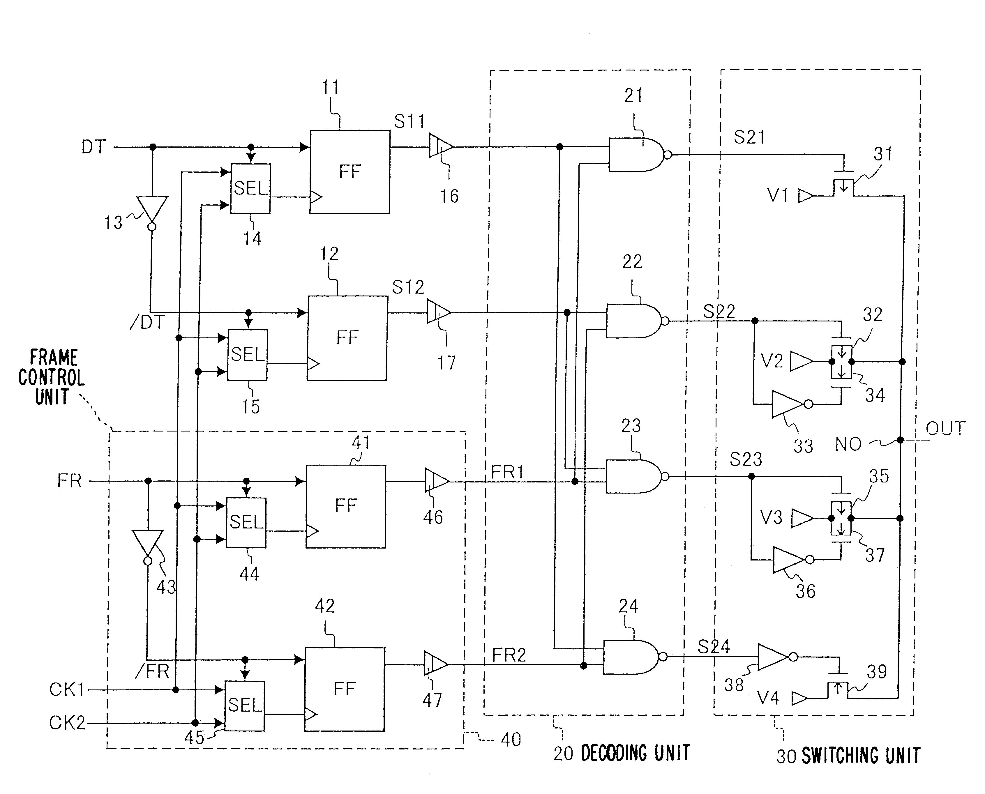
FIG. 2 is a circuit diagram of a driving circuit showing a first embodiment of the present invention.

The driving circuit drives segment electrodes in, for example, a matrix type LCD and has holding circuits (e.g., FFs) 11 and 12 for holding an input signal (e.g., display data) DT corresponding to one segment electrode. The display data DT is supplied to an input terminal of the FF 11. Display data / DT inverted by an inverter 13 is supplied to an input terminal of the FF 12. A clock signal selected by selecting circuit (for example, a selector (SEL)) 14 is supplied to a clock terminal of the FF 11 and a clock signal selected by a selector 15 is supplied to a clock terminal of the FF 12. A clock signal CK1 and a clock signal CK2 delayed in phase relative to the signal CK1 are supplied to two input terminals of each of the selectors 14 and 15. The display data DT is supplied to a control terminal of the selector 14 and the display data / DT is supplied to a control terminal of the selec...

second embodiment

FIGS. 5, 6A and 6B are circuit diagrams regarding a driving circuit showing a second embodiment of the present invention. FIG. 5 shows a circuit construction, FIG. 6A shows the construction of an inverter for PMOS control, and FIG. 6B shows the construction of an inverter for NMOS control. Referring to FIG. 5, components common to those in FIG. 2 are designated by the common reference numerals and symbols.

As shown in FIG. 5, the driving circuit includes holding circuits (for example, FFs) 51, 52, 53, and 54 for holding selection signals DS1, DS2, DS3, and DS4 for selecting a driving voltage for display in accordance with the rising of the common clock signal CK. The selection signals DS1 to DS4 are signals corresponding to the driving voltages V1 to V4, respectively. Each signal is obtained by decoding, for example, the display data DT and the frame control signal FR in FIG. 2. Any one of the selection signals becomes the level "H" and the other signals go to the level "L".

Outputs o...

third embodiment

FIG. 7 is a circuit diagram of a driving circuit showing a third embodiment of the present invention. Components common to those in FIG. 5 are designated by the same reference numerals and symbols.

The driving circuit uses the two-phase clock signals CK1 and CK2, similar to FIG. 2, instead of the clock signal CK in FIG. 5 and has selecting circuits (for example, selectors) 55 to 58 for switching one of the clock signals CK1 and CK2 to the other one and supplying it to the holding circuits (for example, FFs) 51 to 54. The selectors 55 to 58 are similar to the selectors 14 and 15 in FIG. 2. Each selector selects one of the clock signals CK1 and CK2 in accordance with the level "L" or "H" of the signal supplied to the control terminal and generates the selected clock signal.

In the driving circuit, normal inverters 81, 82, and 83 are used instead of the inverters 71, 72, and 75 for PMOS control in FIG. 5, the inverters 73, 74, 76, 78, and 79 in FIG. 5 are eliminated, the outputs of the l...


PUM

PropertyMeasurementUnit
driving voltagesaaaaaaaaaa
voltageaaaaaaaaaa
timeaaaaaaaaaa

Abstract

A driving circuit includes a driving signal generating circuit which generates a plurality of driving signals; a plurality of switching circuits which are supplied with the driving signals so as to supply driving voltages in response to the driving signals, respectively; an output node which is connected to each of the switching circuits and is supplied with one of the driving voltages selectively; and a control circuit which controls the switching circuits so that any two of the switching circuits are not turned on simultaneously.

Description

This application claims the priority of Application No. 2000-354113, filed Nov. 21, 2000 in Japan, the subject matter of which is incorporated herein by reference.The present invention relates to a driving circuit for driving an LCD (liquid crystal display) or the like.A conventional driving circuit is designed to drive segment electrodes in, for example, a matrix type LCD. According to a conventional driving circuit, a leakage current may flow between driving voltages via an output node. Although the leakage current caused in each driving circuit is small, as the number of driving circuits is increased in association with a trend toward a larger screen of the LCD, the total power consumption is increased. The increase in power consumption associated with the trend toward the larger screen is a serious problem especially in battery-powered portable displays.OBJECTS OF THE INVENTIONAccordingly, it is an object of the present invention to provide a driving circuit in which the problem...

Claims


Application Information

Patent Timeline
Patent Type & Authority Patents(United States)
IPC IPC(8): G09G3/36G09G3/20G02F1/133H03K17/16H03K17/687H03K19/0175
CPCG09G3/3685
Inventor NITAWAKI, SHOUJI
Owner LAPIS SEMICON CO LTD