

Crystal growing device and method of manufacturing single crystal
Inactive Publication Date: 2003-05-13
JX NIPPON MINING& METALS CORP +1
View PDF5 Cites 6 Cited by
- Summary
- Abstract
- Description
- Claims
- Application Information
AI Technical Summary
Benefits of technology
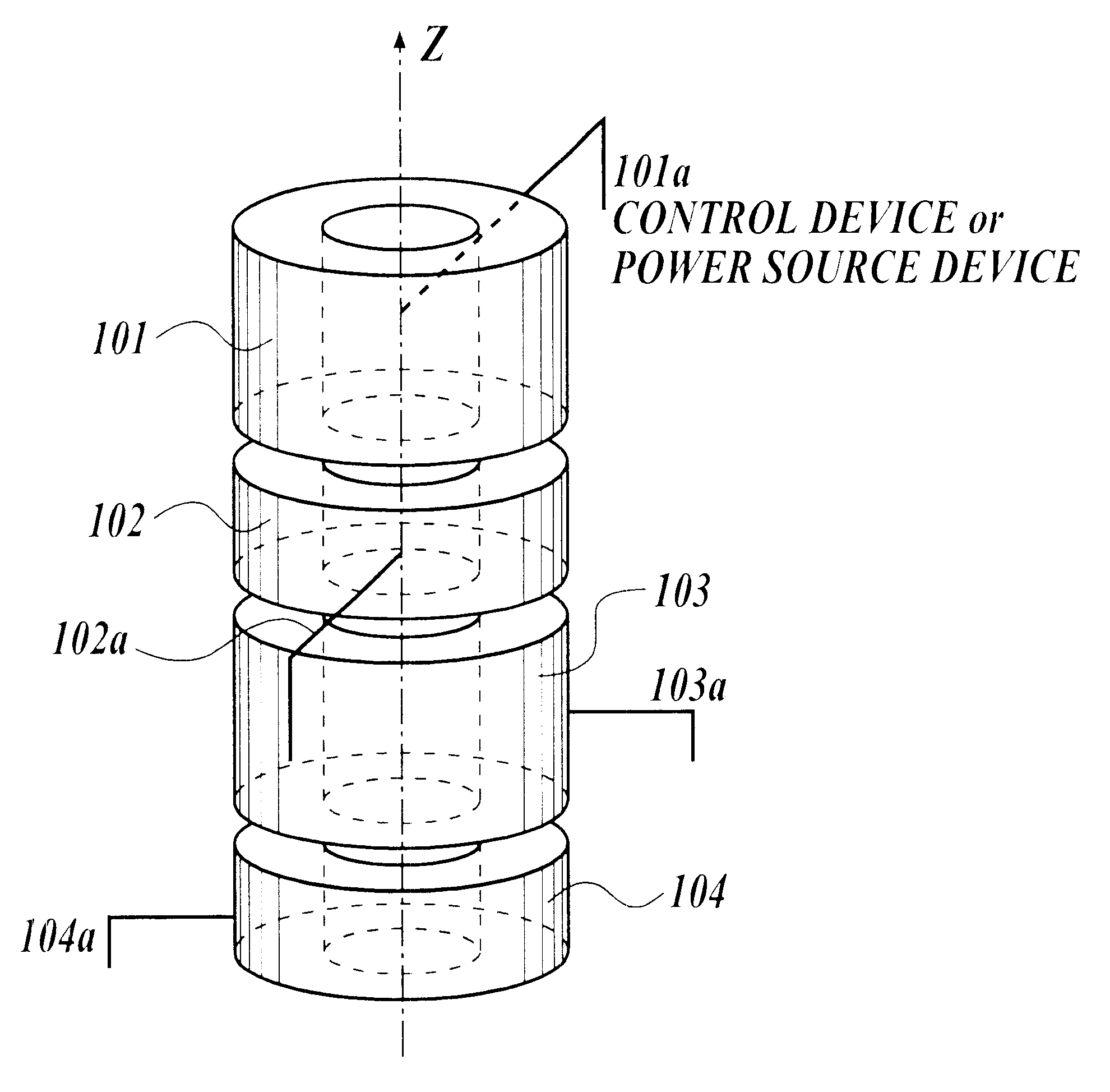
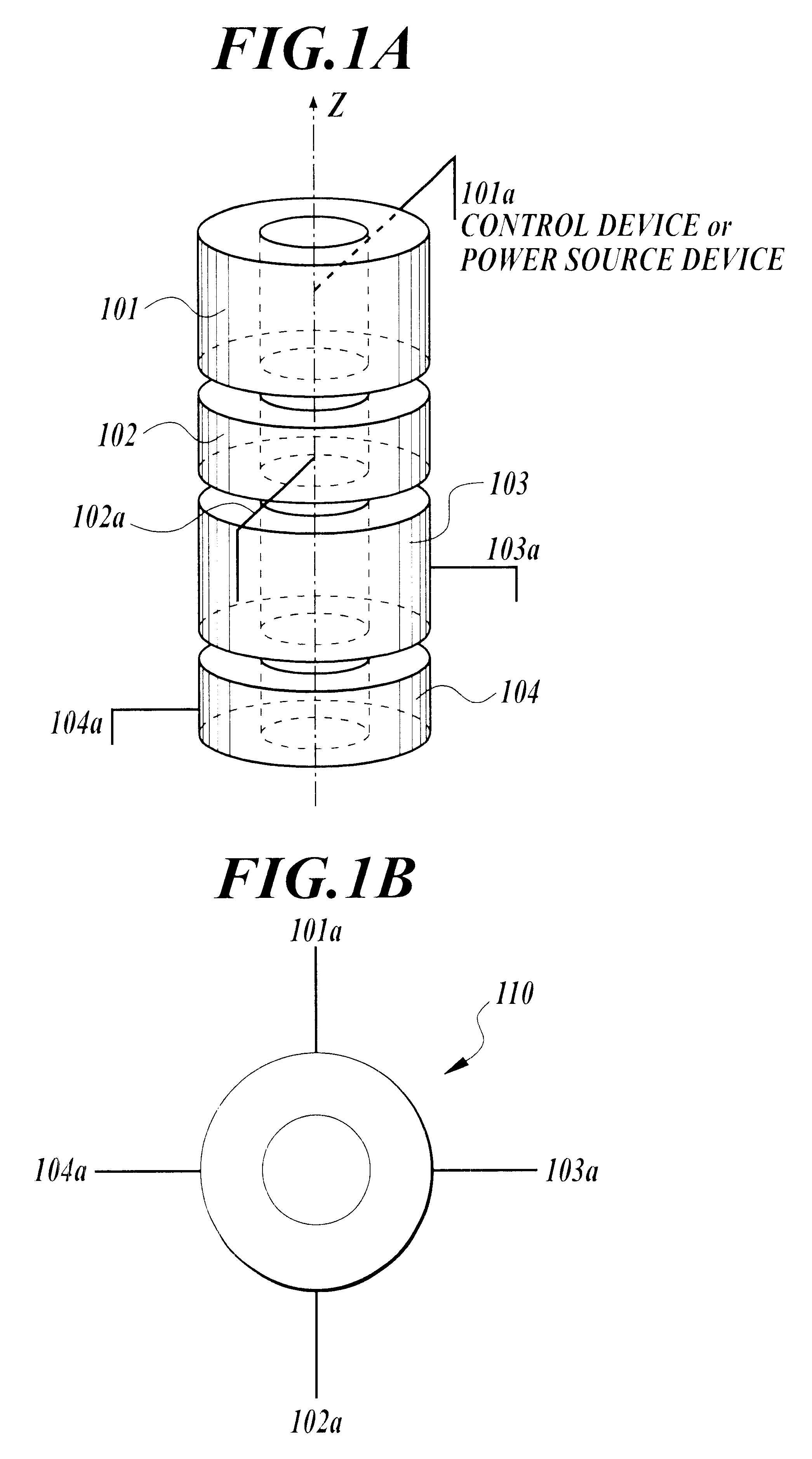
Concretely, when the number of the heaters is, for example, two, each heater may be disposed so that the terminals may be located at an almost facing position. Further, when the number of the heaters is N (N is a positive integer of three or more), each heater may be disposed so that the terminal portions of the heaters may be located at each apex of a regular n-gon (n is an integer which satisfies 3.ltoreq.n.ltoreq.N), seeing from the axial direction of the heating furnace. Therefore, since heat radiation from the terminal portions does not occur at one place, it is possible to uniform the inplane temperature distribution in the heating furnace.
In order to grow a single crystal by using the crystal growth apparatus, for example, a heat-resistant container charged with a raw material is disposed in the heating furnace portion of the crystal growth apparatus. The heater is controlled and a predetermined temperature distribution is made in the furnace. Then, after melting the raw material by heating the heat-resistant container portion to be over the melting point of the raw material, the crystal is grown preferably by decreasing the temperature of the heating furnace gradually, while maintaining the temperature distribution. Thereby, the uniformity of the inplane dopant concentration of a wafer obtained can be improved sharply.
Further, a crystal growth apparatus of a compound semiconductor comprises a heating furnace having an upper stage heater portion heating a crucible portion charged with a raw material of a compound semiconductor, and a lower stage heater portion heating a reservoir portion communicated with a quartz ampoule sealing the crucible. The upper stage heater portion is constituted of N numbers of heaters, which are laminated in multi-stage in an axial direction. Each heater is disposed in order for the terminal portion of each heater in the upper stage heater portion to be located at each apex of a regular N-gon, seeing from the axial direction of the heating furnace. Moreover, each heater may be disposed in order for the terminal portion of each heater in the upper stage heater portion to draw a spiral along the external
Problems solved by technology
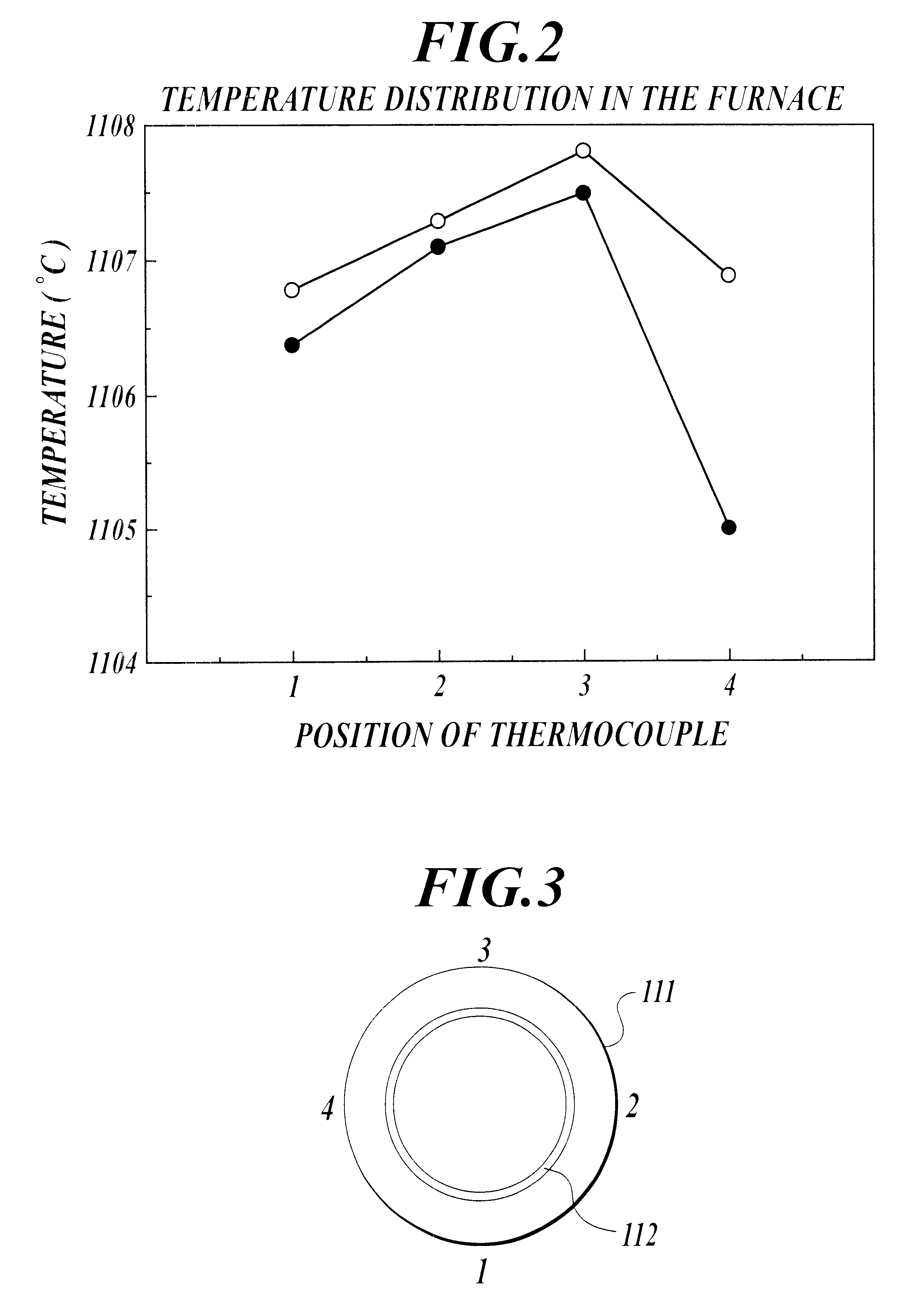
However, in growth of a compound semiconductor single crystal by using the above-described crystal growth apparatus having a multi-stage heater, although it is possible to improve the yield of a single crystal substrate, when aiming at an inplane dopant (impurity) concentration of a obtained wafer, it was found by an experiment that there is dispersion at least beyond the measurement error in a plane.
Therefore, it is ascer
Method used
View moreImage
Smart ImageViewing Examples

Examples
 PUM
 Abstract
A crystal growth apparatus comprising a heating furnace capable of controlling uniformly the temperature distribution in the same horizontal plane, and a method for producing a single crystal by using the crystal growth apparatus are provided. In the crystal growth apparatus comprising a cylindrical heating furnace (110) having plural heaters (101, 102, 103 and 104) laminated in multi-stage in an axial direction (Z), each heater is disposed for the terminal portions of the adjacent heaters not to be overlapped in the same position, but to be in a mutually separated position, seeing from the axial direction of the heating furnace. Concretely, in case of N (n is a positive integer of three or more) heaters, each heater (101, 102, 103 and 104) is disposed for the terminal portions (110a, 102a, 103a and 104a) of the heaters to be located at each apex of a regular n-gon (n is an integer satisfying 3<=n<=N), seeing from the axial direction Z of the heating furnace.
Description
The present invention relates to a crystal growth apparatus comprising a heating furnace, which has a multi-stage heater. Particularly, it relates to a crystal growth apparatus of a compound semiconductor that requires a precise temperature control, and to an effective technology applied to a crystal growth method by using the crystal growth apparatus.Generally, the vertical gradient freezing (VGF) method, vertical Bridgman (VB) method, horizontal gradient freezing (HGF) method and horizontal Bridgman (HB) method or the like have been known as methods for growing a compound semiconductor single crystal. In these methods, a compound semiconductor single crystal is grown by utilizing the temperature gradient in a growth furnace.In a crystal growth apparatus to which such a growth method is applied, in order to realize the desired temperature gradient, there is a case that a heating furnace having a multi-stage heater is used. As an invention using a heating furnace having a multi-stag...
Claims
Login to View More Application Information
Patent Timeline
 IPC IPC(8): C30B11/00
CPCC30B11/00C30B11/003C30B29/48Y10T117/1088Y10T117/1096
InventorMAEDA, HIROSHIHIRANO, RYUICHIYAMAMOTO, TETSUYAHICHIWA, AKIRAKUBOTA, YOSHIAKI
OwnerJX NIPPON MINING& METALS CORP