MIS transistor and method for making same on a semiconductor substrate

a technology of semiconductor substrates and transistors, which is applied in the direction of transistors, semiconductor/solid-state device manufacturing, electric devices, etc., can solve the problems of low threshold voltage of transistors, and low efficiency of transistors,

Inactive Publication Date: 2003-05-13
COMMISSARIAT A LENERGIE ATOMIQUE ET AUX ENERGIES ALTERNATIVES
View PDF10 Cites 87 Cited by
  • Summary
  • Abstract
  • Description
  • Claims
  • Application Information

AI Technical Summary

Benefits of technology

This property makes it possible to adjust the threshold voltage of the transistor, by controlling the doping. It also makes it possible to raise the immunity of the transistor to a drain-source drilling, and above all to reduce the parasite capacities between the channel and the source and drain regions.
Furthermore, thanks to the partial elimination of the pedestal layer under the spacers, the gate extends partly over the source and drain regions. When the source and drain are doped gradually, that is to say with a weakly doped zone turned towards the channel and a more highly doped zone turned away from the channel respectively, the edges of the gate extend as far as above the weakly doped zones. Such an architecture makes it possible to produce a good compromise between reduction of the resistance of access to the channel and reduction of channel-source and channel-drain parasite capacities.
The aim of the oxide layer is not only to increase the thickness of the spacers on the sides of the well but also to control this thickness precisely in such a way as to define a very thin doped zone at the centre of the channel.
By controlling the extension of the zone in this way, by oxidation of the spacers, it is possible to adjust the threshold voltage Vt of the transistor precisely.
When there is total or partial elimination of the pedestal layer in the well, the lateral spacers formed on the sides of the well also have the function of protecting these sides and in this way avoiding any widening of the well, which would prejudice the compactness of the transistor.
Thus, after this stage, and before putting the definitive gate into place, one can form a new oxide layer on the spacers. This measure makes it possible to adjust or exaggerate the upside-down T shape of the gate.

Problems solved by technology

For cost reasons, the circuits produced on gallium arsenide substrates are in general not very complex and do not have a high density of integration.
The architecture of these circuits is thus not optimised from the point of view of their compactness.
When the size of the gate is reduced, there are problems of adjustment of the threshold voltage of transistors and problems of drilling between drain and source.
When the dimensions of the gate are reduced, the doping increases in the channel and it become more difficult to optimise the frequency performances of the components.
One of the limitations of frequency performance is the channel-source or channel-drain parasite capacity.

Method used


Image

  • MIS transistor and method for making same on a semiconductor substrate
  • MIS transistor and method for making same on a semiconductor substrate
  • MIS transistor and method for making same on a semiconductor substrate

Examples


Embodiment Construction

An aim of the present invention is to propose an MIS transistor and its manufacturing method which does not have the limitations mentioned above.

A particular aim of the present invention is to propose such a transistor which can be produced with especially reduced dimensions while still possessing good immunity to drilling.

A further aim of the invention is to be able to adjust the threshold voltage Vt of the transistor to a required value, chosen in function of the supply voltage.

A final aim of the invention is to propose a transistor with low parasite capacities and able to operate at high frequencies.

In order to achieve these aims, the Invention has more precisely the aim of a method for manufacturing an MIS transistor on a semiconductor substrate. The method comprises the following successive stages:

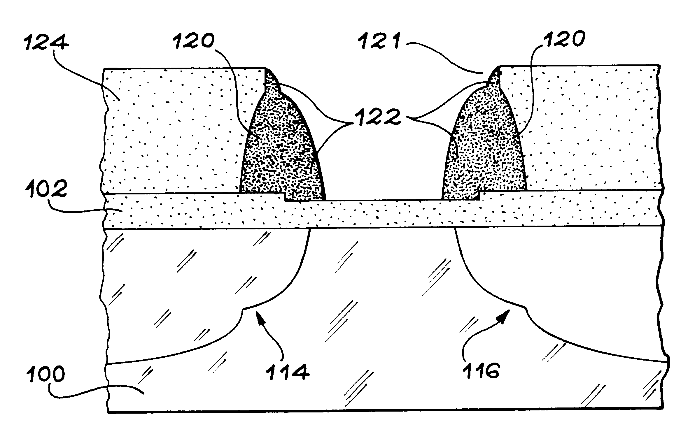
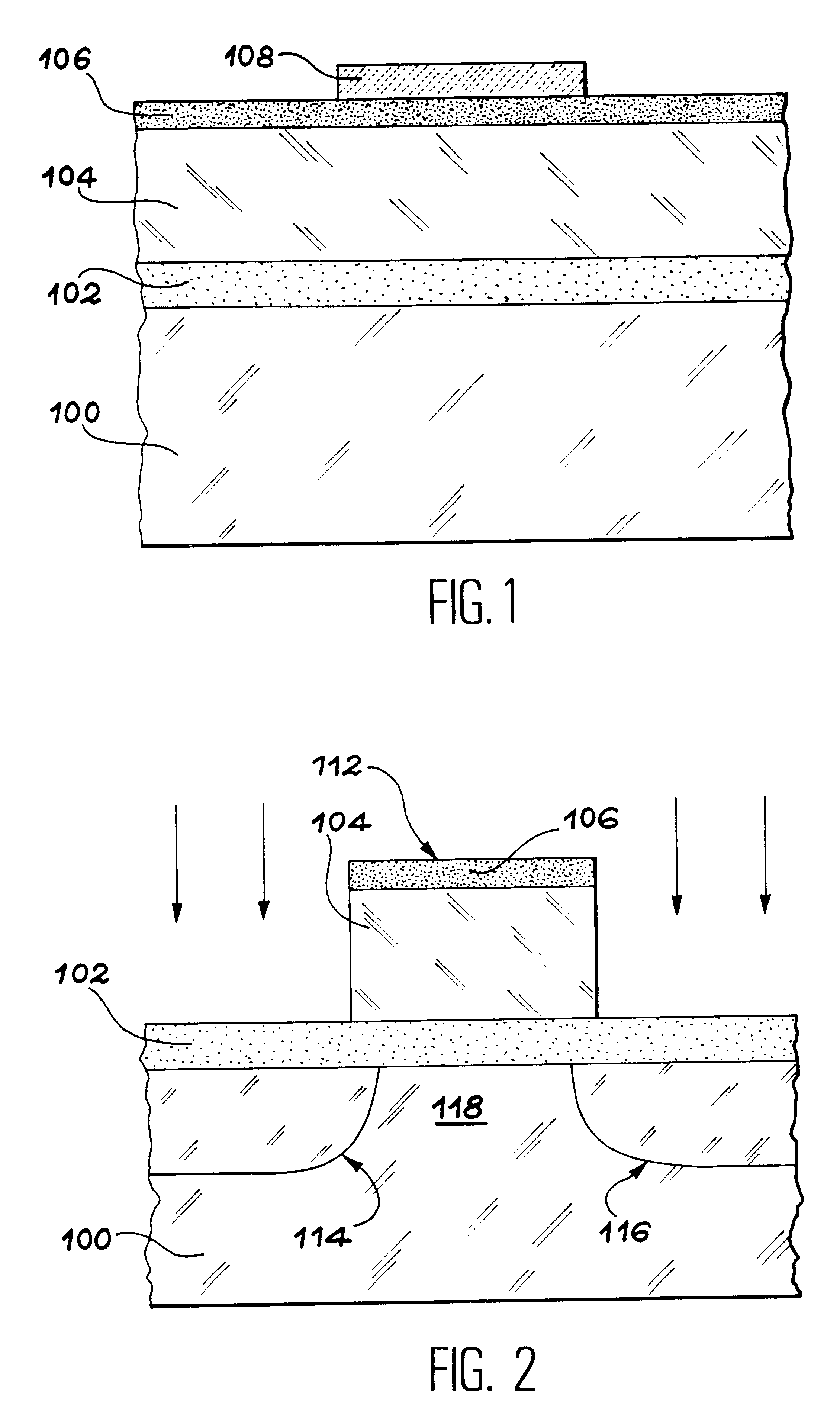
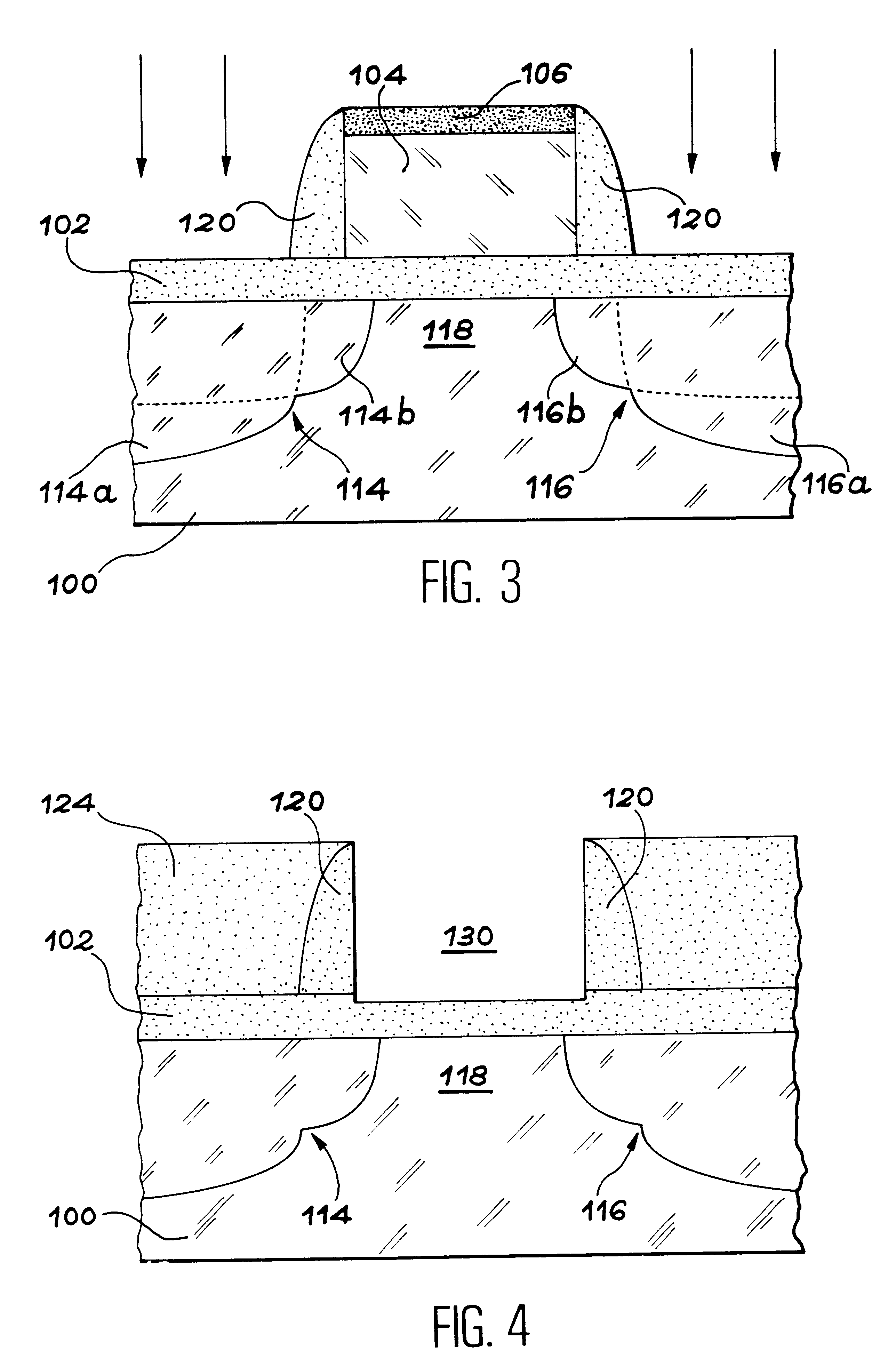
a) formation on the substrate of a layer, called the pedestal layer and, on this layer, formation of a sacrificial dummy gate, the dummy gate being set above a region of the substrate...


PUM


Abstract

The invention relates to an MIS transistor comprising a channel region (118), source (114) and drain (116) regions arranged on either side of the channel, and a gate (150) set closely above the channel region. According to the invention, the channel has a doped central part (140), located between the source and drain regions, and separated from said source and drain regions.

Description

The present invention relates to an MIS transistor with self-aligned gate and its manufacturing method. An MIS transistor refers to a structure of Metal-Insulator-Semiconductor type such as, for example, that of MOS transistors (Metal-Oxide-Semiconductor).In particular the invention relates to the manufacture, on a silicon substrate, of such transistors, capable of functioning in the ultra-high frequency ranges.The invention can be applied to micro-electronics for manufacturing ultra-high frequency and / or power circuits, for example for producing circuits which can be used in the domain of telecommunications.STATE OF PRIOR ARTIt is known that the components and circuits of the ultra-high frequency type are usually produced on substrates in gallium arsenide (GaAs) or on silicon substrates (Si).For cost reasons, the circuits produced on gallium arsenide substrates are in general not very complex and do not have a high density of integration. The architecture of these circuits is thus ...

Claims


Application Information

Patent Timeline
Patent Type & Authority Patents(United States)
IPC IPC(8): H01L21/02H01L21/28H01L29/10H01L21/336H01L29/02H01L29/423H01L29/40H01L29/78H01L29/66H01L29/41H01L29/43H01L29/49
CPCH01L21/28035H01L21/28079H01L21/28088H01L21/28114H01L29/1045H01L29/66537H01L29/66545H01L29/66553H01L29/6659H01L29/42376H01L29/7836
Inventor DELEONIBUS, SIMONGUEGAN, GEORGESCAILLAT, CHRISTIANCOUDERT, FABIEN
Owner COMMISSARIAT A LENERGIE ATOMIQUE ET AUX ENERGIES ALTERNATIVES
Why Eureka
Try Eureka