Wavelength conversion apparatus using semiconductor optical amplifying element for laser oscillation

a technology of optical amplifier and wavelength conversion, which is applied in the direction of optical resonator shape and construction, semiconductor laser, instruments, etc., can solve the problems of mode hopping, light output power fluctuation, and unignorable nois

Inactive Publication Date: 2003-05-27
FUJIFILM HLDG CORP +1
View PDF4 Cites 6 Cited by
  • Summary
  • Abstract
  • Description
  • Claims
  • Application Information

AI Technical Summary

Problems solved by technology

However, since mode control is insufficient in the wide-beam semiconductor laser device, mode hopping occurs.
Therefore, light output power fluctuates even under a constant driving current, and an unignorable amount of noise (represented by a ratio of RF noise intensity and DC noise intensity of the optical output) is produced.
In addition, due to the noise of the semiconductor laser device, the output laser light having the wavelength of 946 nm also includes noise.
Further, due to the mode hopping in the wide-beam semiconductor laser device, wavelengths of a portion of the output laser light of the wide-beam semiconductor laser device are not within the absorption band of the YAG crystal, and such a portion of the laser light also increases noise.
Furthermore, the noise in the laser light of 946 nm causes noise in the blue light output from the wavelength conversion element.
Further, since the laser optical crystals utilize transitions in doped rare earth elements, only limited wavelengths can be obtained from the laser optical crystals.
In addition, since the optical output of the semiconductor laser device becomes a broadened longitudinal mode, the output optical power varies due to mode competition.
Thus, according to the conventional technique, the modulated, wavelength-converted light cannot be made stable and the conventional wavelength conversion apparatuses are not efficient.
As described above, since the conventional wavelength conversion apparatuses use laser optical crystals having narrow absorption bands, output light of excitation light sources cannot be utilized efficiently, and noise is produced.
Therefore, the conventional wavelength conversion apparatuses are not suitable for obtaining stable optical output on a long-term basis.
In addition, according to the conventional wavelength conversion apparatuses, obtainable wavelengths are limited by the laser optical crystals used in the wavelength conversion apparatuses, and therefore it is impossible to obtain an arbitrary wavelength in the visible and ultraviolet ranges.

Method used


Image

  • Wavelength conversion apparatus using semiconductor optical amplifying element for laser oscillation
  • Wavelength conversion apparatus using semiconductor optical amplifying element for laser oscillation
  • Wavelength conversion apparatus using semiconductor optical amplifying element for laser oscillation

Examples


first embodiment

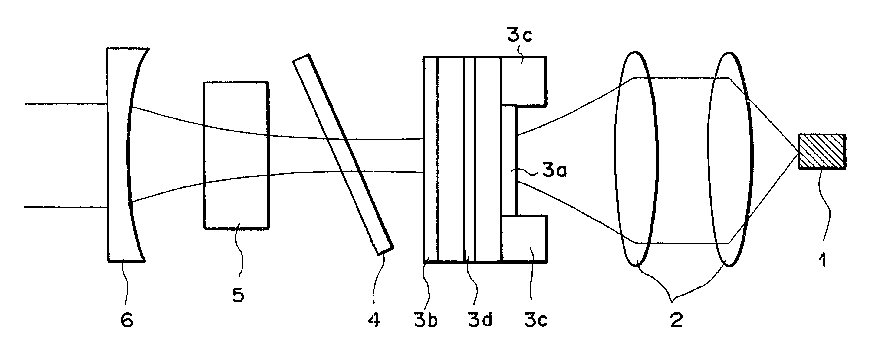
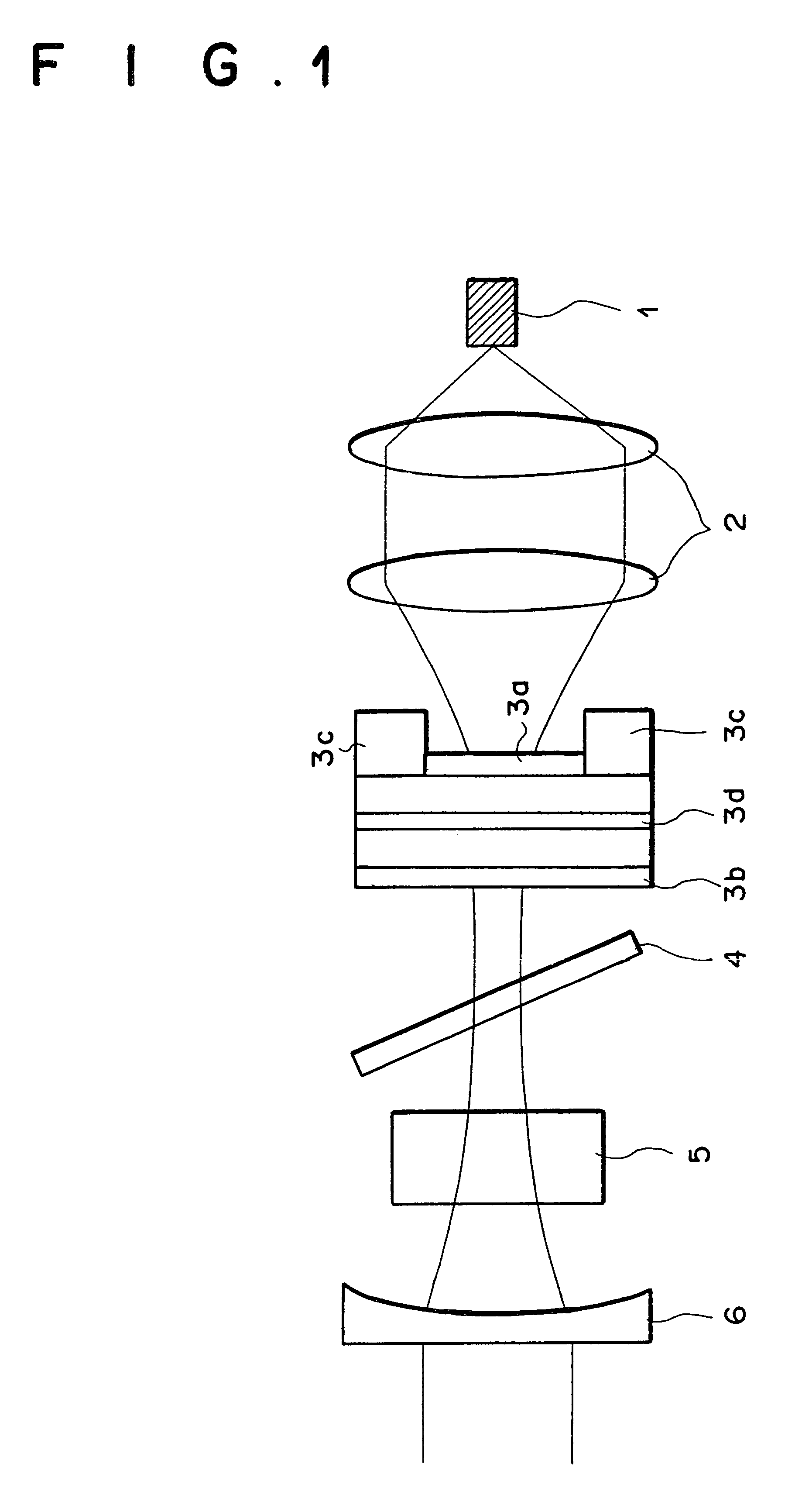
FIG. 1 is a diagram illustrating the construction of the wavelength conversion apparatus as the first embodiment of the present invention. In the construction of FIG. 1, excitation laser light is supplied to the back end surface of the semiconductor optical amplifying element.

As illustrated in FIG. 1, the excitation laser light emitted by the semiconductor laser device 1 (as an excitation light source) is collected and converged by the lens system 2, and enters the active layer 3d of the semiconductor optical amplifying element 3 from the back end surface in the direction perpendicular to the substrate 3c thereof. Excited by the excitation laser light, the semiconductor optical amplifying element 3 emits laser light. The laser light emitted by the semiconductor optical amplifying element 3 passes through the birefringent filter 4 and the wavelength conversion element 5, and reaches the concave mirror 6. The birefringent filter 4 is provided for controlling the longitudinal mode of t...

second embodiment

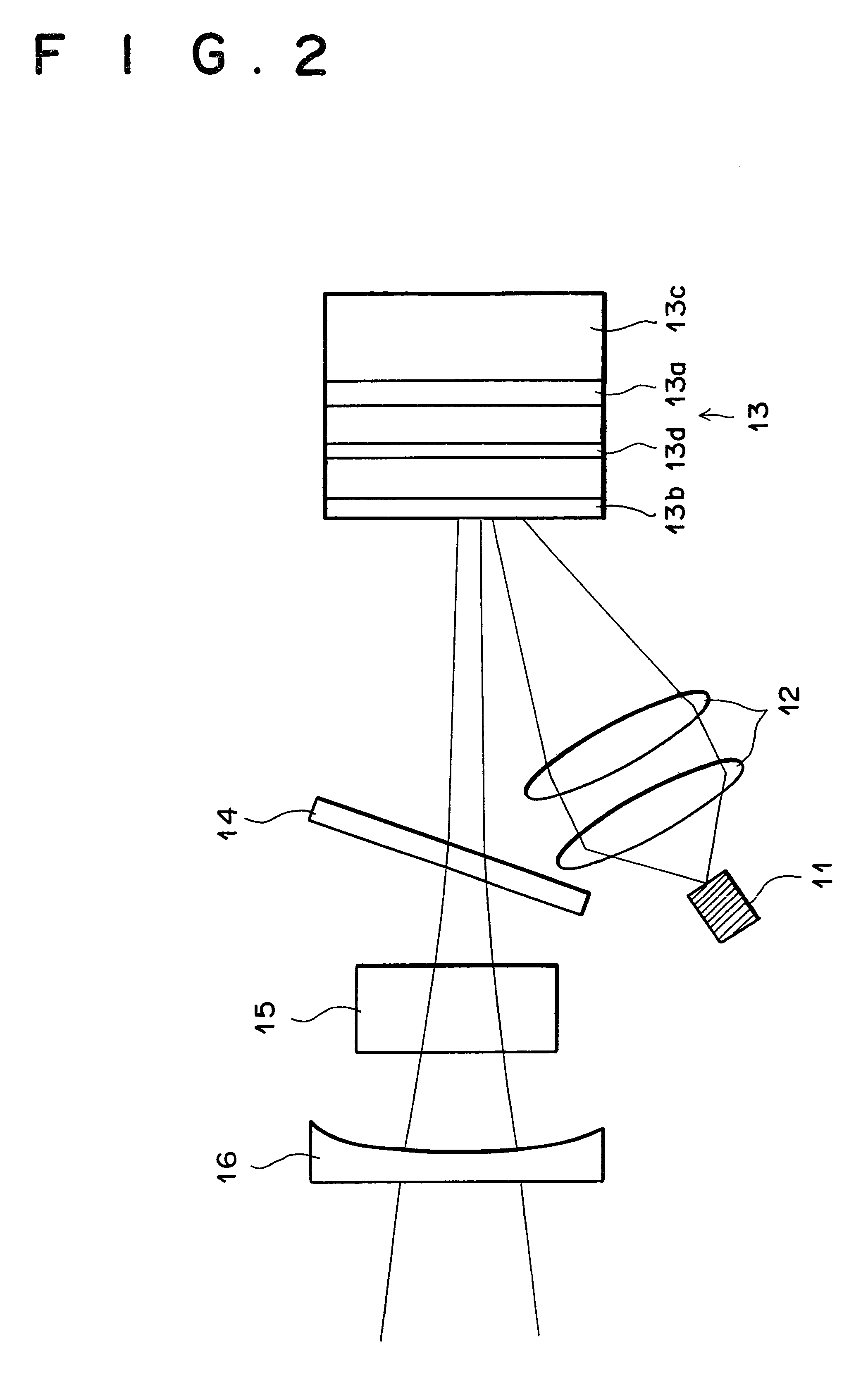
FIG. 2 is a diagram illustrating the construction of the wavelength conversion apparatus as the second embodiment of the present invention. In the construction of FIG. 2, excitation laser light enters the semiconductor optical amplifying element from a surface through which laser light generated by the semiconductor optical amplifying element exits from the semiconductor optical amplifying element.

As illustrated in FIG. 2, the excitation laser light emitted by the semiconductor laser device 11 (as an excitation light source) is collected and converged by the lens system 12, and enters the active layer 13d of the semiconductor optical amplifying element 13 through the periodic-structure dielectric film 13b, where the incident angle of the excitation laser light on the periodic-structure dielectric film 13b is exactly or nearly the Brewster's angle, i.e., the excitation laser light entering the semiconductor optical amplifying element 13 is substantially p-polarized light. When the in...

third embodiment

FIG. 3 is a diagram illustrating the construction of the wavelength conversion apparatus as the third embodiment of the present invention. In the construction of FIG. 3, excitation laser light from the semiconductor laser device is supplied through a beam splitter to the semiconductor optical amplifying element. The excitation laser light enters the semiconductor optical amplifying element from a surface through which laser light generated by the semiconductor optical amplifying element exits from the semiconductor optical amplifying element.

As illustrated in FIG. 3, the excitation laser light emitted by the semiconductor laser device 21 (as an excitation light source) is collected and converged by the lens system 22, is reflected by the beam splitter 27, and enters the active layer 23d of the semiconductor optical amplifying element 23 through the wavelength conversion element 25 and the periodic-structure dielectric film 23b in the direction perpendicular to the substrate 23c of t...


PUM

PropertyMeasurementUnit
stripe widthaaaaaaaaaa
reflectanceaaaaaaaaaa

Abstract

A wavelength conversion apparatus contains a semiconductor laser device as an excitation light source, a semiconductor optical amplifying element, a resonator formed by the optical amplifying element and a mirror arranged outside the optical amplifying element, and a wavelength conversion element arranged in the resonator. The semiconductor laser device emits excitation laser light which is supplied to the semiconductor optical amplifying element. The semiconductor optical amplifying element has an active layer on a substrate thereof, and is excited by the excitation laser light to emit laser light. Then, the laser light emitted by the semiconductor optical amplifying element is converted by the wavelength conversion element to reduce the wavelength to half.

Description

1. Field of the InventionThe present invention relates to a wavelength conversion apparatus which uses a wavelength conversion element and a semiconductor laser device as an excitation light source.2. Description of the Related ArtConventional wavelength conversion apparatuses use laser optical crystals such as Nd-doped YAG, Nd-doped YVO.sub.4, Nd-doped YLF, or the like. Each of the laser optical crystals is excited by a semiconductor laser device which emits laser light having a wavelength band broader than an absorption band of the laser optical crystal, and a wavelength of the laser light emitted by the laser optical crystal is converted by a nonlinear crystal or a wavelength conversion element such as domain-inverted LiNbO.sub.3. As a result of the conversion, for example, the wavelength of the laser light emitted by the laser optical crystal is reduced to half.Typically, a laser optical crystal of YAG is excited by excitation laser light having a wavelength of 809 nm, which is ...

Claims


Application Information

Patent Timeline
Patent Type & Authority Patents(United States)
IPC IPC(8): H01S5/04H01S5/14H01S5/00H01S5/06G02F1/37H01L33/32H01L33/44H01L33/50H01L33/60H01S5/323
CPCH01S5/14H01S5/041H01S3/109H01S5/141
Inventor MIZUYOSHI, AKIRA
Owner FUJIFILM HLDG CORP
Why Eureka
Try Eureka