Device for multiplexing/demultiplexing and method therewith

a technology of multiplexing and multiplication, applied in multiplex communication, electromagnetic repeaters, instruments, etc., can solve the problems of large losses and instabilities, large energy consumption of devices, and large loss of devices,

Inactive Publication Date: 2003-05-27
TELEFON AB LM ERICSSON (PUBL)
View PDF6 Cites 14 Cited by
  • Summary
  • Abstract
  • Description
  • Claims
  • Application Information

AI Technical Summary

Benefits of technology

It is in this respect a particular object of the invention to provide such a device that exhibits better filter profiles and a lower channel crosstalk.
The advantages of the present invention are principally that the device is compact and thereby admits a short propagation path for the light. Thus, lower losses and stability against temperature gradients are achieved. Further, the invention shows a flexible functionality, provides possibilities for creating improved performance and that it in some respects exhibits more system tolerant properties in comparison with known art, which uses linear phase responses.

Problems solved by technology

Generally, the problems of the above known techniques comprise a long propagation path for the light through the respective device, which gives rise to large losses and instabilities.
Further, to tune (phase control) the device relatively high energy consumption is needed.
Further, known techniques may give problems with channel crosstalk and need relatively complicated structures.

Method used


Image

  • Device for multiplexing/demultiplexing and method therewith
  • Device for multiplexing/demultiplexing and method therewith
  • Device for multiplexing/demultiplexing and method therewith

Examples


Embodiment Construction

In the following description, with a describing and not limiting purpose, specific details are given, such as particular applications, techniques, methods etc., to provide a thorough understanding of the present invention. It shall, however, be apparent for the man skilled in the art that the invention may be practised in other embodiments that deviate from these specific details. In other instances, detailed descriptions of well-known methods, devices or circuits are omitted so as not to obscure the present description with unnecessary details.

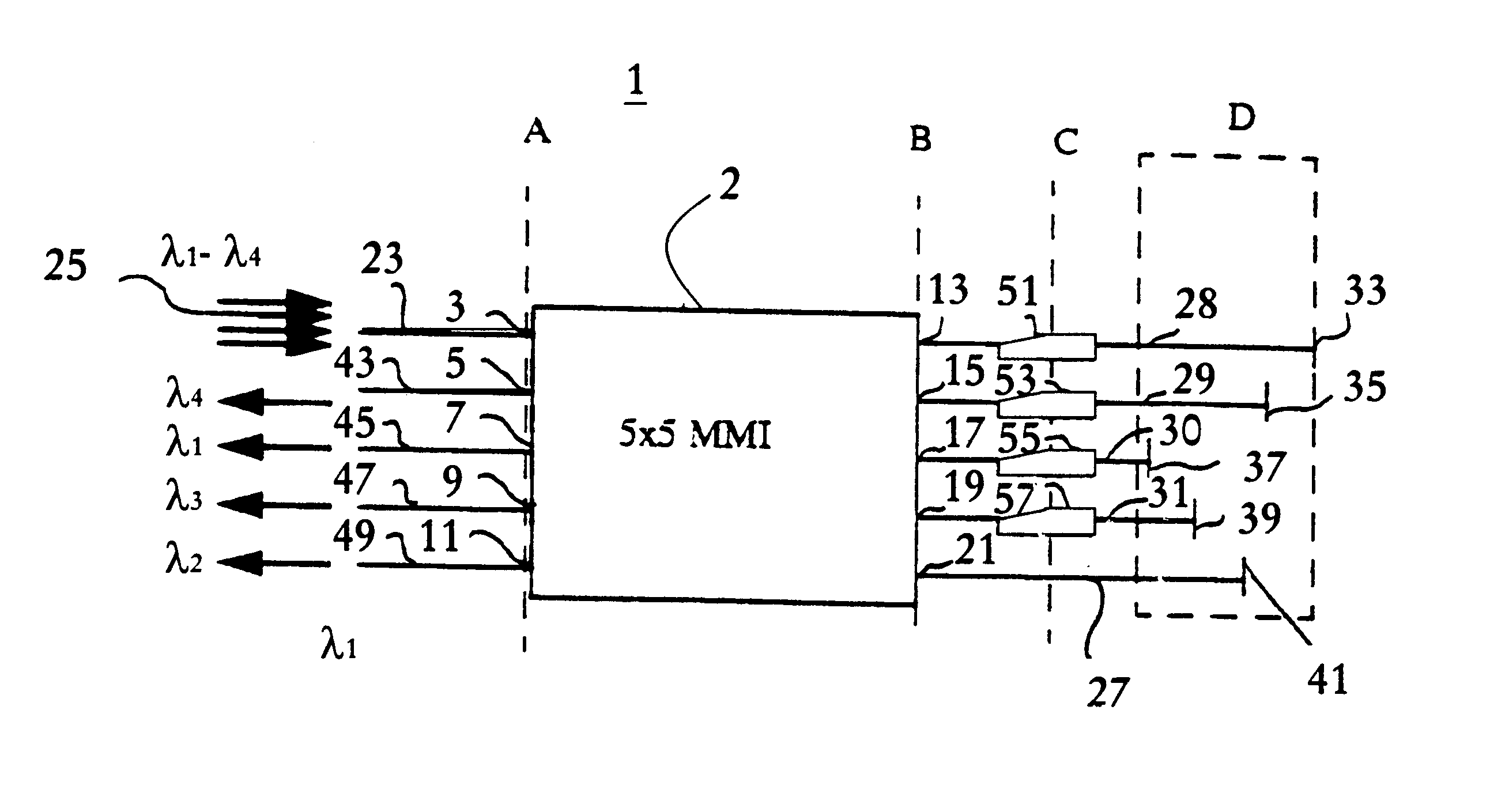
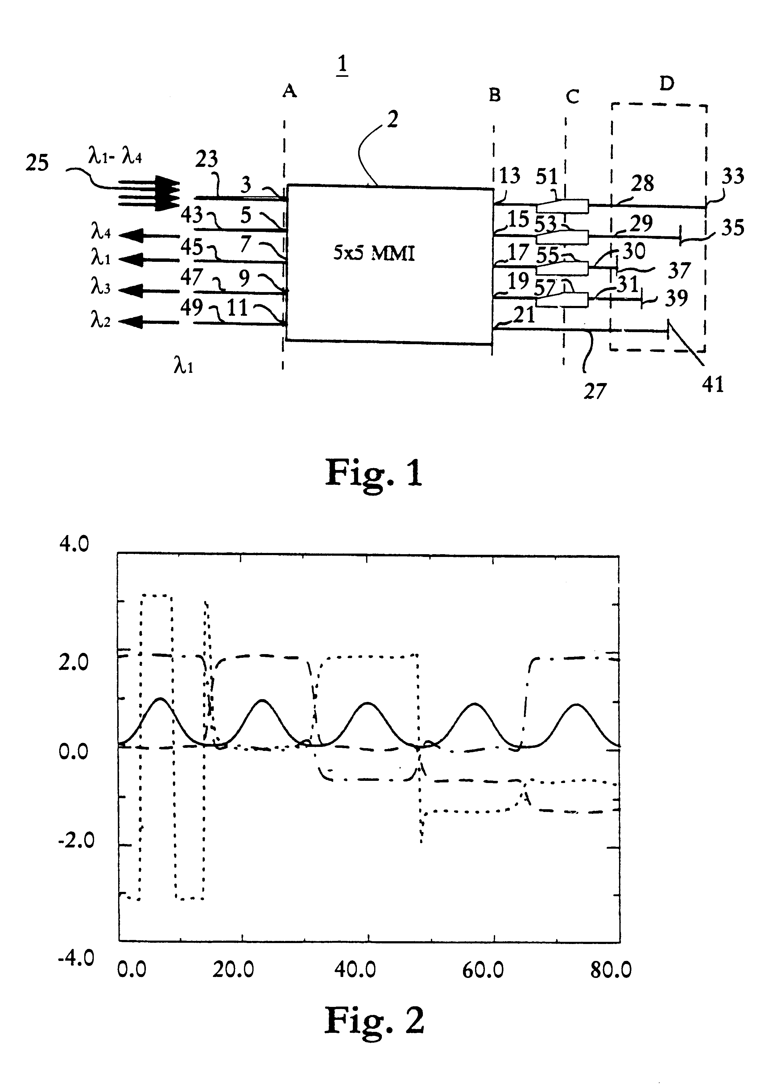
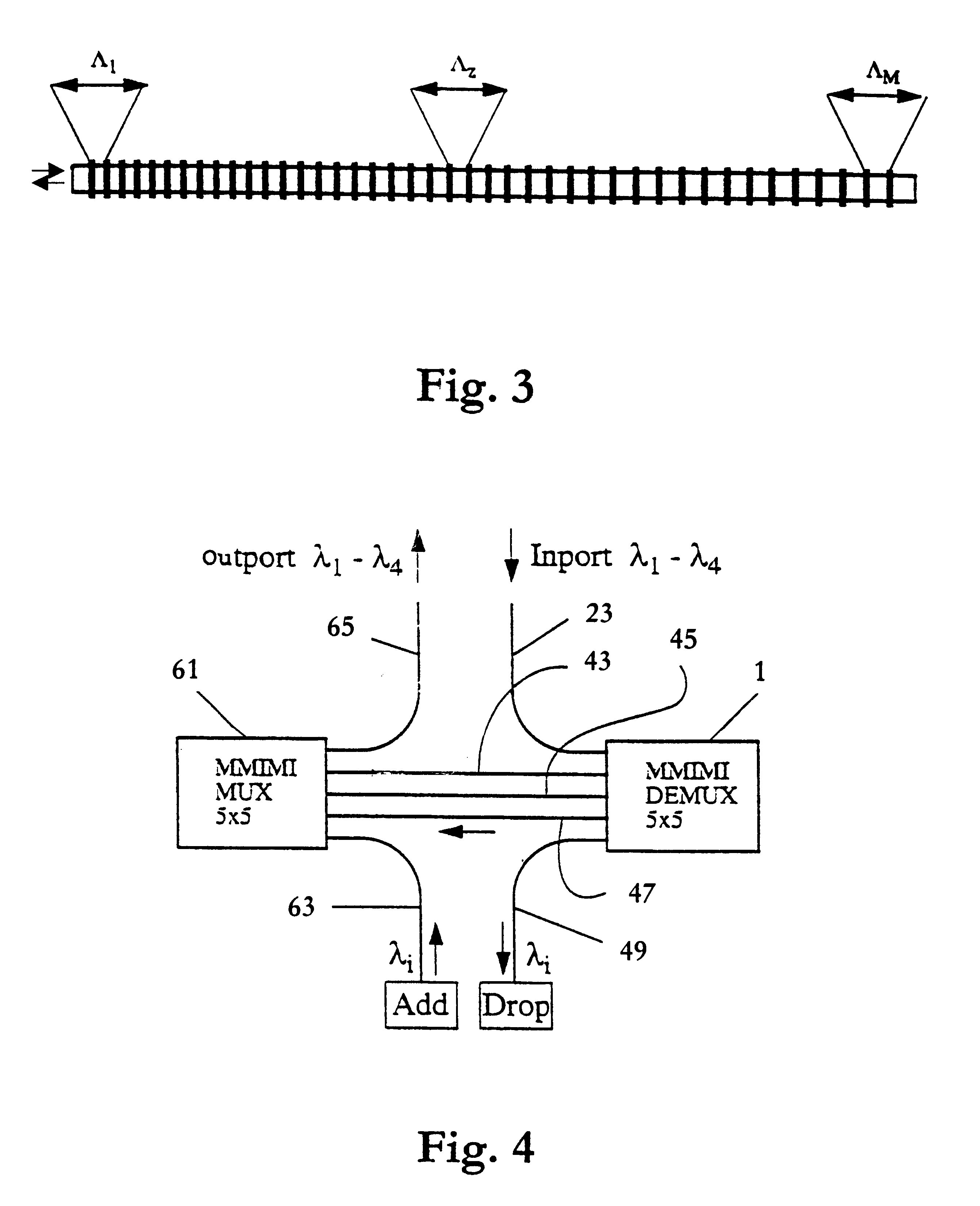
The present invention comprises a new and inventive device for multiplexing / demultiplexing an optical signal comprising an MMI coupler both for splitting the optical signal (in one direction) and for phase dependent combining (in the second direction), i.e. in a Michelson configuration. The reflecting structure, which may be comprised of a Bragg grating, is adapted to achieve a phase relation between the different splitted components for each...


PUM

PropertyMeasurementUnit
wavelengthsaaaaaaaaaa
sizeaaaaaaaaaa
lengthsaaaaaaaaaa

Abstract

A device for multiplexing a wavelength multiplexed optical signal (25) comprising at least a first and a second optical wavelength channel centered around respective predetermined wavelengths (lambd1, lambd2), comprising an MMI coupler (2), at least of the size 2x2, for inputting the wavelength multiplexed optical signal at an input (3) and for splitting the multiplexed signal into components and imaging these at several ports (13-21), Michelson waveguides (27-31) for receiving and transporting the components imaged at the port of the MMI coupler, reflecting means (33-41) for reflecting the components received and transported in the Michelson waveguides back to the ports of the MMI coupler, wherein the MMI coupler is arranged for inputting the reflecting components, and the respective lengths of the Michelson waveguides are adapted so that said MMI coupler combines the components in a manner such that the first and the second optical wavelength channels are imaged substantially at separated outputs (5-11).

Description

BACKGROUND OF THE INVENTION AND RELATED ARTA number of different methods to increase the capacity of optical fibres in a network are known. One of these comprises to utilize wavelength division multiplexing (WDM) in order to improve the utility of bandwidth in the network, which, however, requires provision of devices capable to multiplex and demultiplex transmission channels that are transferred at different, so-called optical carrier wavelengths, in the network.The publication A new type of tunable demultiplexer using a multileg Mach-Zehnder interferometer, J. -P. Weber et al, Proc. ECIO '97 EthE5, Stockholm, pages 272-275, 1997, shows an MMIMZI device 1 (multimode interference Mach-Zehnder interferometer) that may be used for cyclic wavelength selective switching.C. K. Madsen, A multiport frequency band selector with inherently low loss, flat pass bands, and low cross-talk, Photon. Tech. Lett., Vol. 10(12), pages 1766-1768, 1998.WO 98 / 39686 and T. Augustsson, Bragg grating assist...

Claims


Application Information

Patent Timeline
Patent Type & Authority Patents(United States)
IPC IPC(8): G02B6/34G02B6/28H04J14/02G02F1/01G02F1/035G02F1/313H04B10/27H04B10/29H04B10/291
CPCG02B6/12011G02B6/29301G02B6/29349G02B6/29383G02B6/34G02B6/29317G02B6/2813H04J14/0212
Inventor AUGUSTSSON, TORSTEN
Owner TELEFON AB LM ERICSSON (PUBL)
Why Eureka
Try Eureka