Semiconductor wafer support lift-pin assembly

a technology of semiconductor wafers and lift pins, applied in the direction of liquid surface applicators, coatings, chemical vapor deposition coatings, etc., can solve the problems of lift pins binding, integrated circuits have evolved into complex devices, and the size of lift pins is increased, so as to reduce the space required below the support platform, raise and lower semiconductor wafers, and increase the conductance of gases

Inactive Publication Date: 2003-06-03
APPLIED MATERIALS INC
View PDF7 Cites 25 Cited by
  • Summary
  • Abstract
  • Description
  • Claims
  • Application Information

AI Technical Summary

Benefits of technology

A plurality of lift-pin holes extends through the support platform, the base, the substrate support, and circumscribe the centrally disposed recess. Each of the modular lift-pin assemblies respectively extends (i.e., slidably extends) through the plurality of lift-pin holes, and a C-shaped lift-arm assembly disposed below the base engages the plurality of lift-pin assemblies to raise and lower a semiconductor wafer. The lift-arm assembly passes into a slot in the support platform, thus reducing the space required below the support platform to operate the lift-pins. The reduced space requirement allows for the support platform to be positioned closer to a pumping stack and thereby increasing the conductance of gases through the chamber.

Problems solved by technology

Integrated circuits have evolved into complex devices that include millions of transistors, capacitors and resistors on a single chip.
One problem that has been observed is that the lift-pins may bind as they pass through the lift-pin holes in the substrate support.
Another problem is that the increased size in the industry from 200 mm to 300 mm wafers requires redesign of the processing chambers and accordingly, the lift-pin assemblies with regard to their configuration with other components in the substrate support assembly.

Method used


Image

  • Semiconductor wafer support lift-pin assembly
  • Semiconductor wafer support lift-pin assembly
  • Semiconductor wafer support lift-pin assembly

Examples


Embodiment Construction

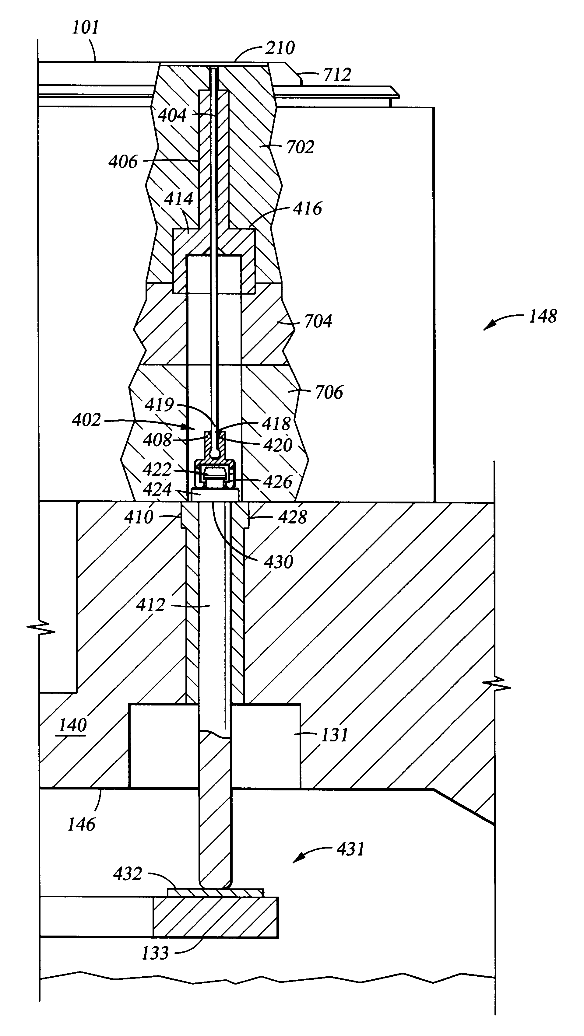
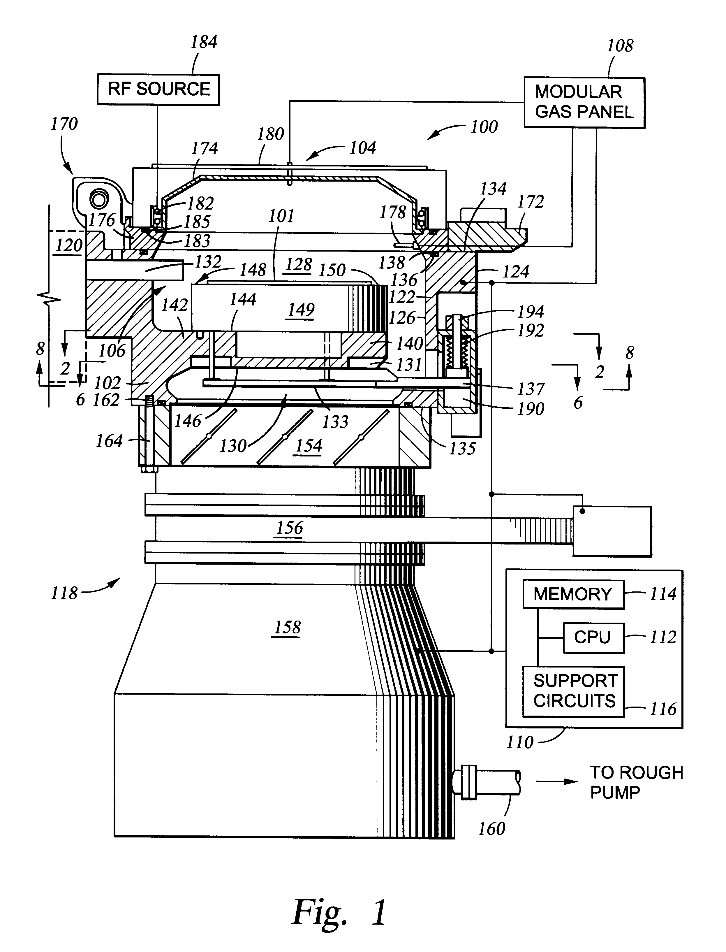
The present invention generally provides an apparatus for processing a semiconductor substrate. The invention is illustratively described below as a chemical vapor deposition system, such as an ULTIMA.RTM. High Density Plasma Chemical Vapor Deposition (HDP-CVD) chamber system, available from Applied Materials, Inc. of Santa Clara, Calif. However, it should be understood that the invention may be incorporated into other chamber configurations such as physical vapor deposition chambers, etch chambers, ion implant chambers, and other semiconductor processing chambers.

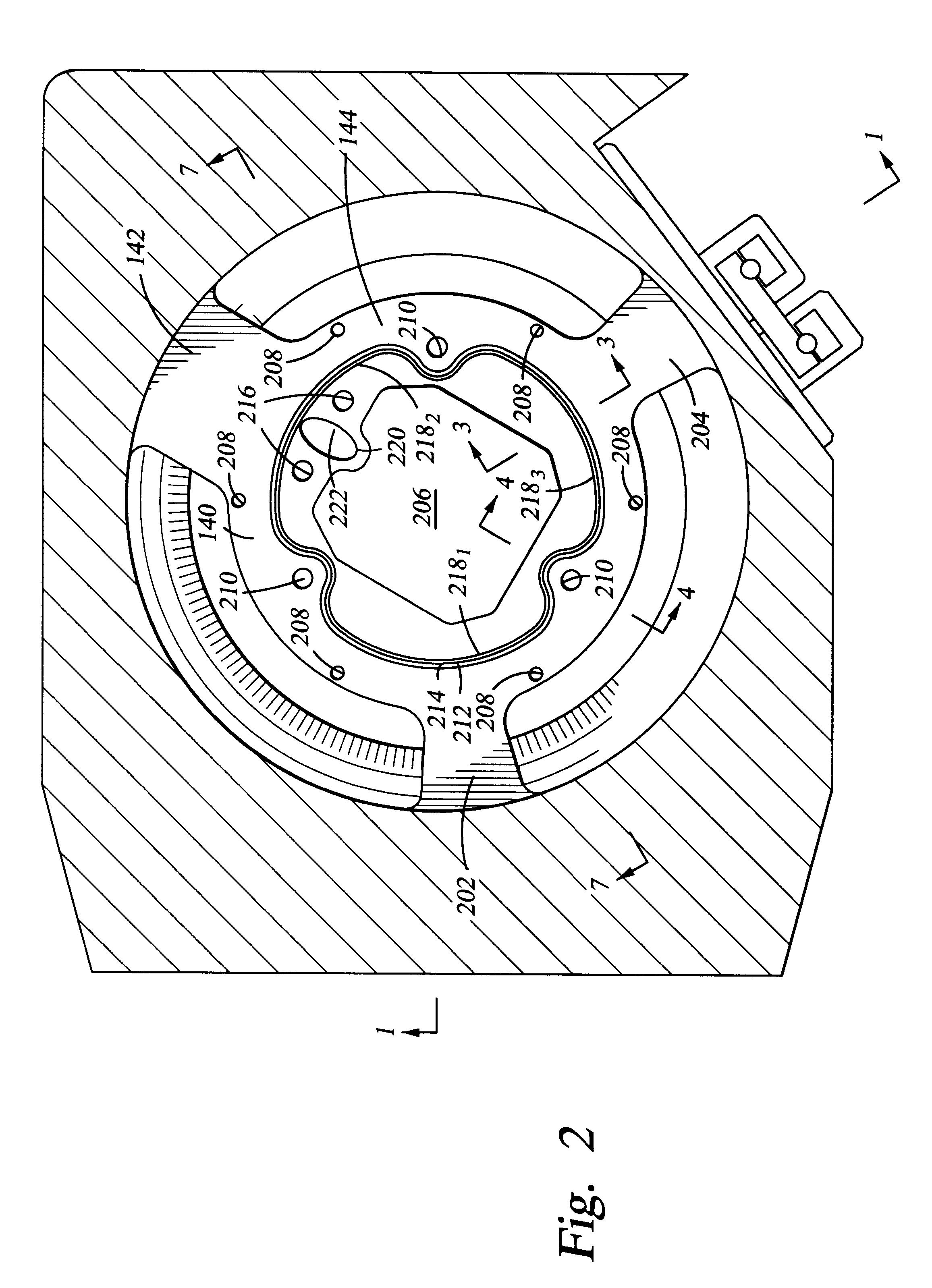
FIG. 1 depicts a cross sectional view of a semiconductor processing system of the present invention. Specifically, FIG. 1 depicts an illustrative HDP-CVD chamber system (system) 100 that generally comprises a chamber body 102 and a lid assembly 104 that defines an evacuable chamber 106 for carrying out substrate processing. The system 100 may be one of a number of substrate processing systems that are coupled to a processi...


PUM

PropertyMeasurementUnit
diametersaaaaaaaaaa
sizeaaaaaaaaaa
diameteraaaaaaaaaa

Abstract

A modular lift-pin assembly comprises a lift-pin having a distal end and a connector having a lift-pin end and an actuator end. The lift-pin end of the connector is coupled to the distal end of the lift-pin and an actuator pin is then coupled to the actuator end of the connector to actuate the lift-pin through the connector.

Description

BACKGROUND OF THE DISCLOSURE1. Field of InventionThe present invention relates generally to an apparatus for processing semiconductor wafers. More specifically, the invention relates to a lift-pin assembly for moving semiconductor wafer using in a semiconductor wafer-processing chamber.2. Description of the Background ArtIntegrated circuits have evolved into complex devices that include millions of transistors, capacitors and resistors on a single chip. The evolution of chip design results in faster circuitry and greater circuit density. As the demand for integrated circuits continues to rise, chip manufactures have demanded semiconductor process tooling having increased wafer throughput and greater product yield. To meet this increase in throughput, tooling is being developed to process wider diameter wafers, for example, wafers having diameters of 300 millimeters (mm).Processing chambers generally capable of processing 300 mm substrates transport and support the substrate by a lif...

Claims


Application Information

Patent Timeline
Patent Type & Authority Patents(United States)
IPC IPC(8): C23C16/458C23C16/44C23C16/40
CPCC23C16/405C23C16/4401C23C16/4586C23C16/4412C23C16/45561C23C16/4409
Inventor GUJER, RUDOLFCHO, THOMAS K.PANG, LILY L.KARAZIM, MICHAEL P.ISHIKAWA, TETSUYA
Owner APPLIED MATERIALS INC
Why Eureka
Try Eureka