

Solar cell device
a solar cell and device technology, applied in the field of solar cell devices, can solve the problems of high cost of forming rough shapes, poor reproducibility of rough shapes, and increase in the total cost of substrates
- Summary
- Abstract
- Description
- Claims
- Application Information
AI Technical Summary
Benefits of technology
Problems solved by technology
Method used
Image

Examples
first embodiment
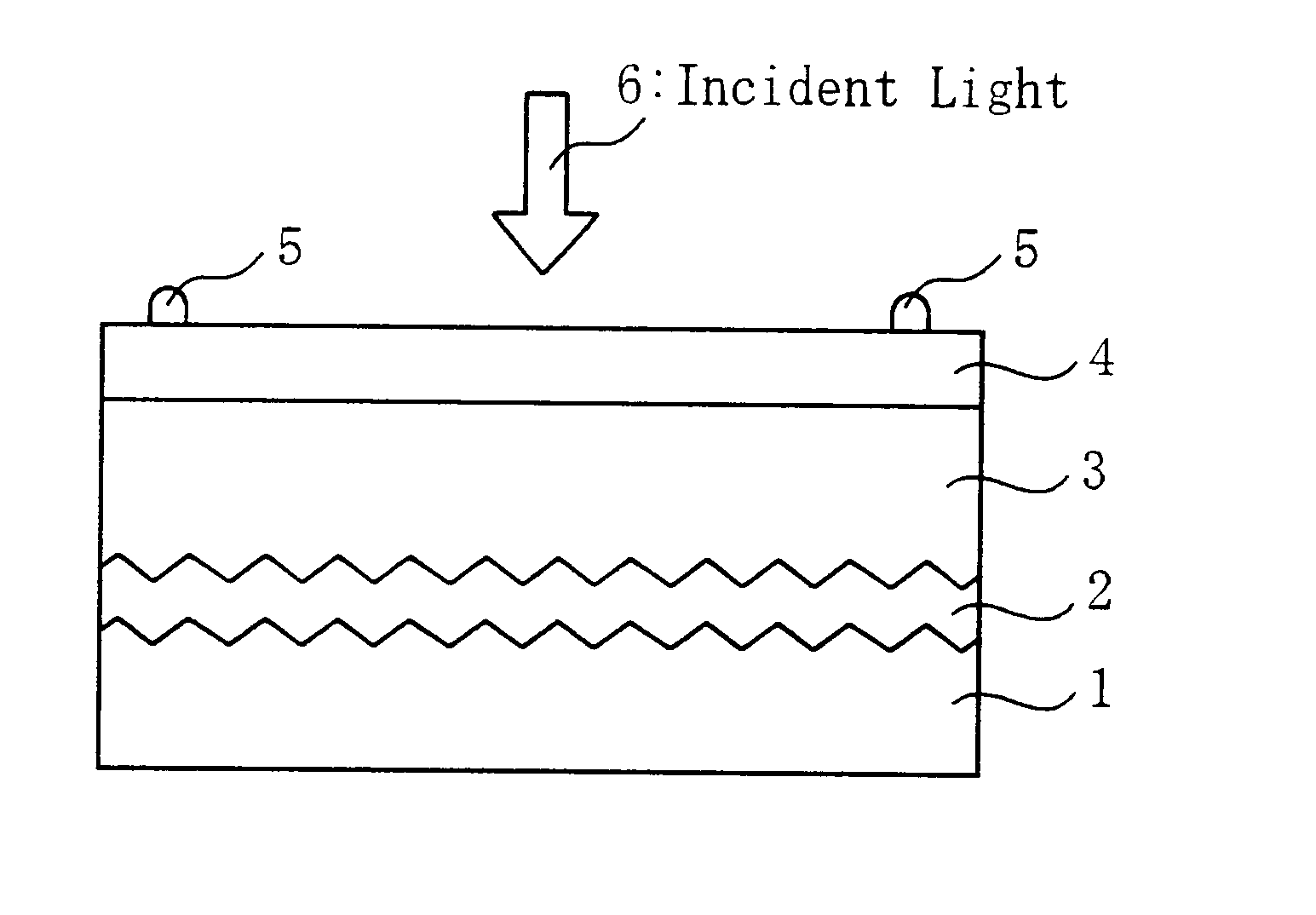
FIG. 1 is a cross sectional view illustrating a structure of a thin film solar cell device of the invention. A substrate 1 is a metal foil of copper, nickel, iron or the like of 10-500 .mu.m in thickness produced by electroforming or a metal foil of alloy of these material. The substrate 1 used in this embodiment is an electroformed copper foil.
"Wet processing handbook" (FOUNDATION ADVANCED TECHNOLOGY INSTITUTE, published on Mar. 22, 1996, 108-123 pages) describes on electroforming, for example. In general, a drum is dipped in an electrolyte bath, metal is deposited on the drum to be thick, and then the electrically deposited material is peeled from the drum to produce into product or duplicate. In manufacturing a copper foil by electroforming, copper electrolyte used in electroforming is acid copper-sulfate containing copper-sulfate of 200 g / l. A drum of titan, stainless steel or the like is partially dipped in the electrolyte bath filled with the acid copper-sulfate, and electrica...
second embodiment
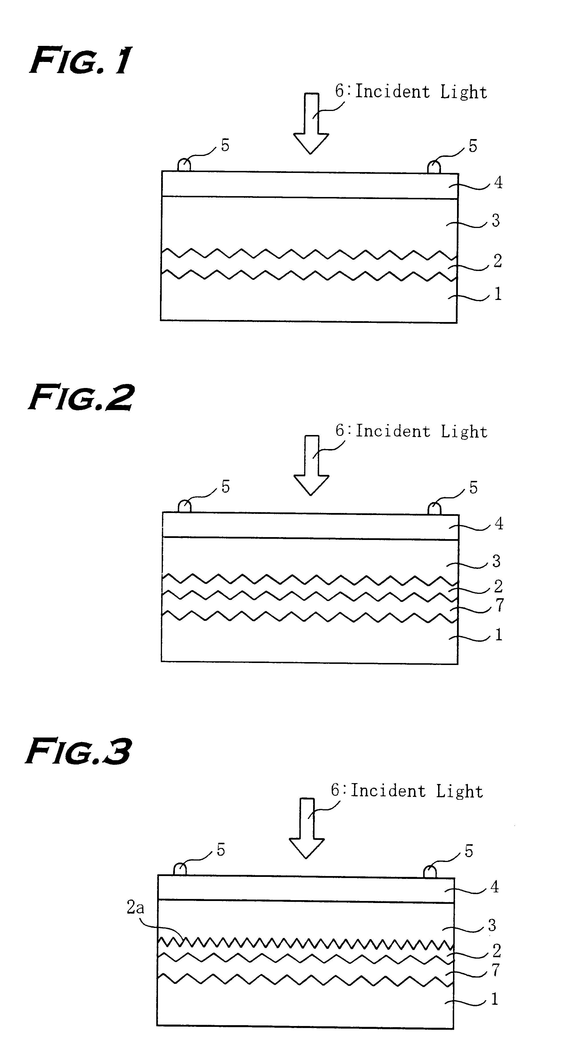
The metal layer of high optical reflectivity of the second embodiment is formed by coating silver (Ag) of 3000 .ANG. in thickness on the rough metal foil substrate 1 by radio frequency (RF) sputtering. The silver is formed under the conditions of argon (Ar) gas atmosphere, reaction pressure of 0.399 Pa, radio frequency power density of 3 W / cm.sup.2, a substrate temperature of room temperature.
Then a transparent conductive material layer 2 of such as tin oxide, indium tin oxide, and zinc oxide is coated on the metal layer 7 by sputtering.
Then, a photovoltaic conversion layer 3 of a thin film semiconductor layer mainly containing amorphous silicon or the like is formed on the transparent conductive material layer 2. As like in the first embodiment, an n-type layer of amorphous silicon layer of 200 .ANG., an i-type layer of amorphous silicon layer of 3000 .ANG., a p-type layer of amorphous silicon carbide layer of 100 .ANG. are laminated in this order from the rough metal foil substrat...
third embodiment
The transparent conductive material layer 2 of the third embodiment is wet-etched by 0.1-2% hydrochloric acid after forming a zinc oxide layer of approximately 0.7-1 .mu.m. The wet-etching can be conducted by using acetic acid aqueous solution other than hydrochloric acid and dipping the layer in it for 10-60 seconds at a room temperature. The rough shape 2a of the transparent conductive material layer 2 can also be formed by dry etching and ion etching.
The transparent conductive material layer 2 of such as tin oxide, indium tin oxide, and zinc oxide having a fine rough shape formed on the metal foil substrate 1 enables to utilize incident light such as sunlight so as to improve efficiency of the solar cell.
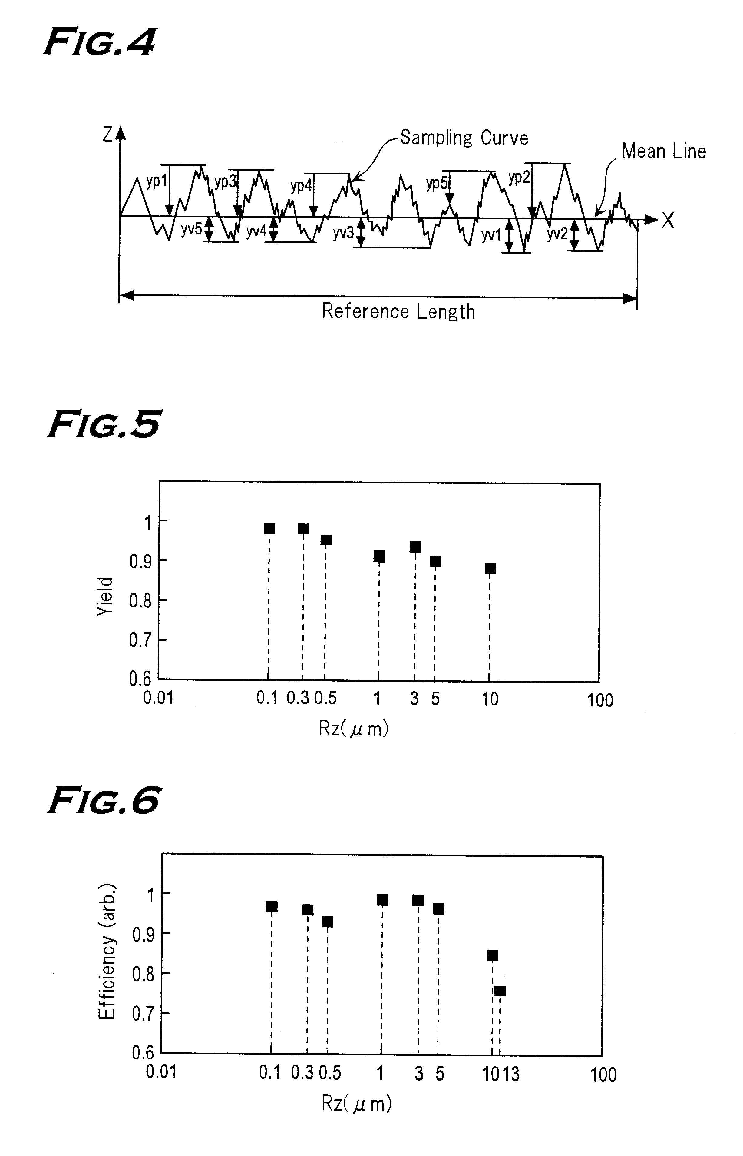
Then, characteristics of the thin film solar cells of the first-third embodiments and a thin film solar cell of a conventional structure are compared. For the thin film solar cell of the conventional structure, a substrate of a glass coated with tin oxide (SnO.sub.2) of a rough s...
PUM
| Property | Measurement | Unit |
|---|---|---|
| mean roughness depth | aaaaa | aaaaa |
| mean roughness depth | aaaaa | aaaaa |
| mean roughness depth | aaaaa | aaaaa |
Abstract
Description
Claims
Application Information