Anti-fuse circuit and method of operation

a technology of anti-fuse circuit and anti-fuse, which is applied in the direction of emergency protective circuit arrangement, and emergency protection arrangement for limiting excess voltage/current, etc., and can solve the problems of difficulty in blowing the fuse, difficulty in using copper fuses, and difficulty in ensuring that the entire copper line has been completely opened

Inactive Publication Date: 2003-07-22
FREESCALE SEMICON INC
View PDF3 Cites 42 Cited by
  • Summary
  • Abstract
  • Description
  • Claims
  • Application Information

AI Technical Summary

Problems solved by technology

With more modern technology utilizing copper as the interconnect layers, especially at the higher levels in the integrated circuit, there have been found to be difficulties in using copper fuses.
When a laser is utilized to blow a copper fuse at this thicker level, there is some difficulty in blowing the fuse because the laser pulse is absorbed by only the upper portion of the copper, and the rest of the copper is blown by heat from conduction.
Because of the requirement or the result that conduction is involved in blowing the fuse, there have been difficulties in ensuring that the entire copper line has been completely opened.
Another difficulty in blowing copper is that it has a high degree of reflection so that very high intensity is required for the laser.
Inherent in the copper blowing process is that it requires additional expense.
In the case of the salicide covered polysilicon the change in resistance that occurs may be difficult to detect.

Method used


Image

  • Anti-fuse circuit and method of operation
  • Anti-fuse circuit and method of operation

Examples


Embodiment Construction

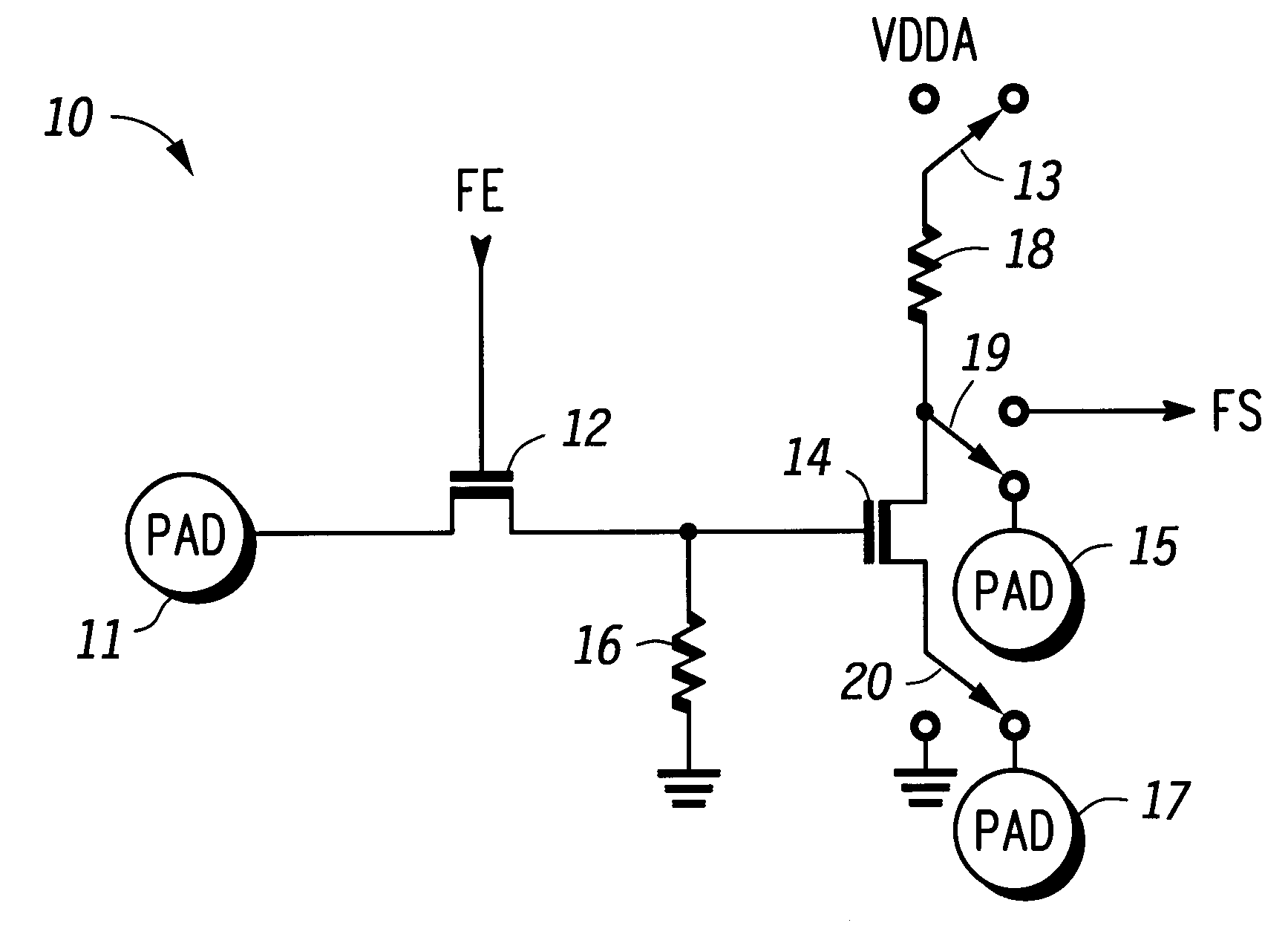
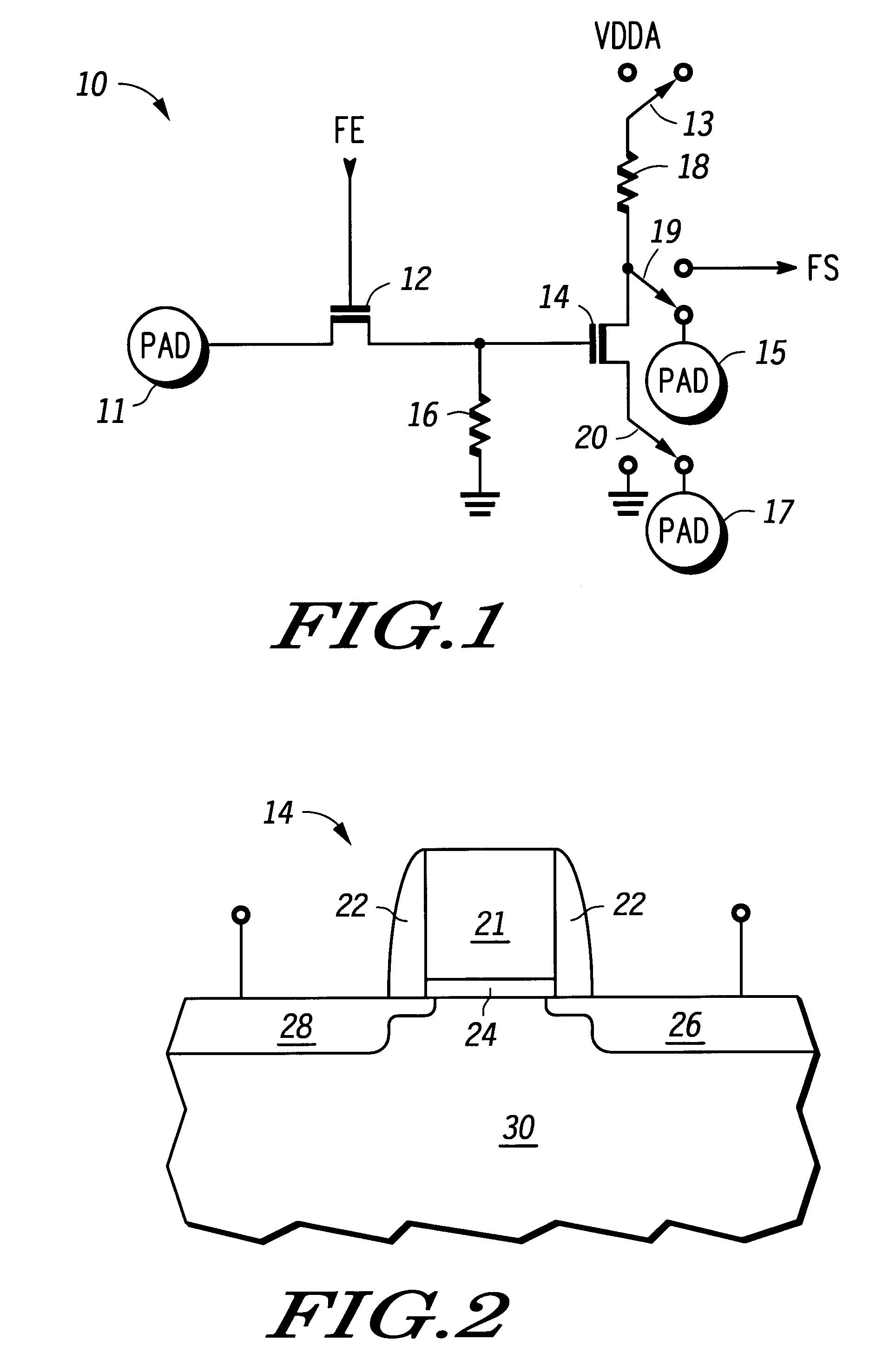
An anti-fuse is achieved by using a fuse transistor as a normal transistor in its non-conductive state as a high impedance state for an un-programmed condition and using the anti-fuse transistor that has had its gate dielectric forced into a conductive condition as a low impedance as the programmed state. This programmed state is achieved by applying a relatively high voltage to the gate of the fuse transistor to cause it to be programmed and thus to be permanently conductive. The anti-fuse transistor is held in a non-conductive condition to provide the un-programmed state. A circuit coupled to the anti-fuse transistor generates a signal to indicate the state of the fuse transistor. This signal can then be used to implement a function such as redundancy in a memory.

Shown in FIG. 1 is an anti-fuse circuit 10 comprising a pad 11, a transistor 12, a switch 13, a transistor 14, a pad 15, a resistor 16, a pad 17, a resistor 18, a switch 19, and a switch 20. Transistor 12 has a gate for r...


PUM


Abstract

An anti-fuse useful in implementing redundancy in a memory utilizes a normal transistor characteristic that is generally considered undesirable in order to provide two easily detected states. The un-programmed state, which is the high impedance state, is achieved simply with a normal transistor in its non-conductive state. The programmed state, which is the low impedance state, is achieved by forcing a normal transistor to conduct current through its gate. This causes the gate dielectric to become permanently conductive. This programmed transistor then is conductive between its source and drain that is easily differentiated from the transistor that is held in its non-conductive state. The result is a fuse technology using an anti-fuse that provides for easily distinguishable programmed and un-programmed states achieved by electrical programming rather than by laser programming.

Description

This invention relates to integrated circuits and more particularly to fusing techniques including anti-fuse circuits useful in integrated circuits.RELATED ARTIt is common in memory integrated circuits to have redundancy that is implemented using fuse technology. The fuse technology is required in order to replace redundant rows or columns with rows and columns from the regular array that have been found to be defective. With more modern technology utilizing copper as the interconnect layers, especially at the higher levels in the integrated circuit, there have been found to be difficulties in using copper fuses. The last layer of copper is typically the thickest. When a laser is utilized to blow a copper fuse at this thicker level, there is some difficulty in blowing the fuse because the laser pulse is absorbed by only the upper portion of the copper, and the rest of the copper is blown by heat from conduction. Because of the requirement or the result that conduction is involved in...

Claims


Application Information

Patent Timeline
Patent Type & Authority Patents(United States)
IPC IPC(8): H01L23/52G11C17/18G11C17/14H01L23/525
CPCG11C17/18H01L23/5252H01L2924/3011H01L2924/0002H01L2924/00
Inventor REBER, DOUGLAS M.CROWN, STEPHEN R.
Owner FREESCALE SEMICON INC
Why Eureka
Try Eureka