Planarization system with multiple polishing pads

a technology of planarization system and polishing pad, which is applied in the direction of lapping machine, manufacturing tools, abrasive surface conditioning devices, etc., can solve the problems of limited conventional planarization system, insufficient pad width, and difficulty in planarizing more than one wafer having a diameter of 300 mm

Inactive Publication Date: 2003-09-30
APPLIED MATERIALS INC
View PDF45 Cites 73 Cited by
  • Summary
  • Abstract
  • Description
  • Claims
  • Application Information

AI Technical Summary

Benefits of technology

In an exemplary embodiment, each polishing head is moved in a polishing pattern comprising a first motion provided by a first linear motion device, and a second motion substantially perpendicular to the first motion pr

Problems solved by technology

One problem common to systems utilizing webs of polishing media is the difficulty in planarizing more than one wafer having a diameter of 300 mm (approximately 1113/16 inches).
This conventional pad width will accommodate a polishing process that positions two 200 mm wafers side-by-side across the width of the pad when polishing, however, this pad width i

Method used


Image

  • Planarization system with multiple polishing pads
  • Planarization system with multiple polishing pads
  • Planarization system with multiple polishing pads

Examples


Embodiment Construction

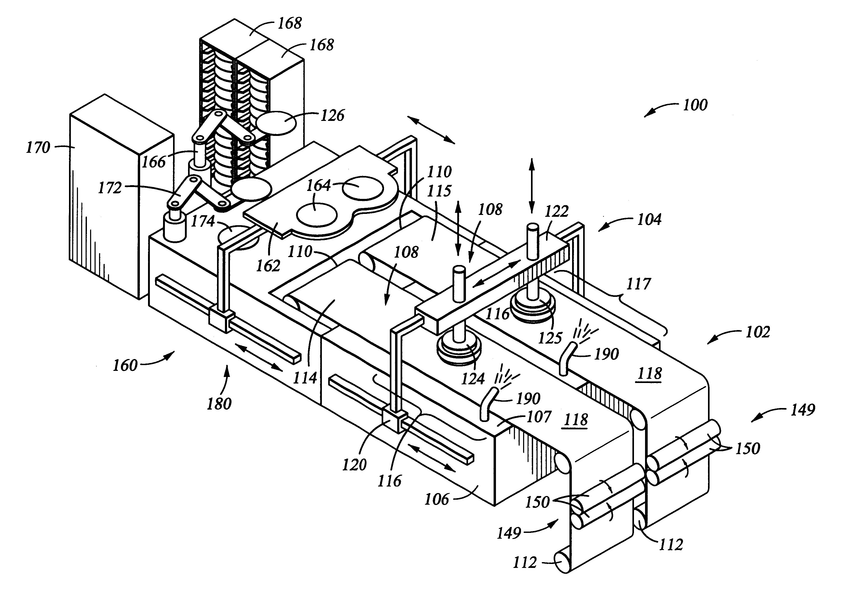
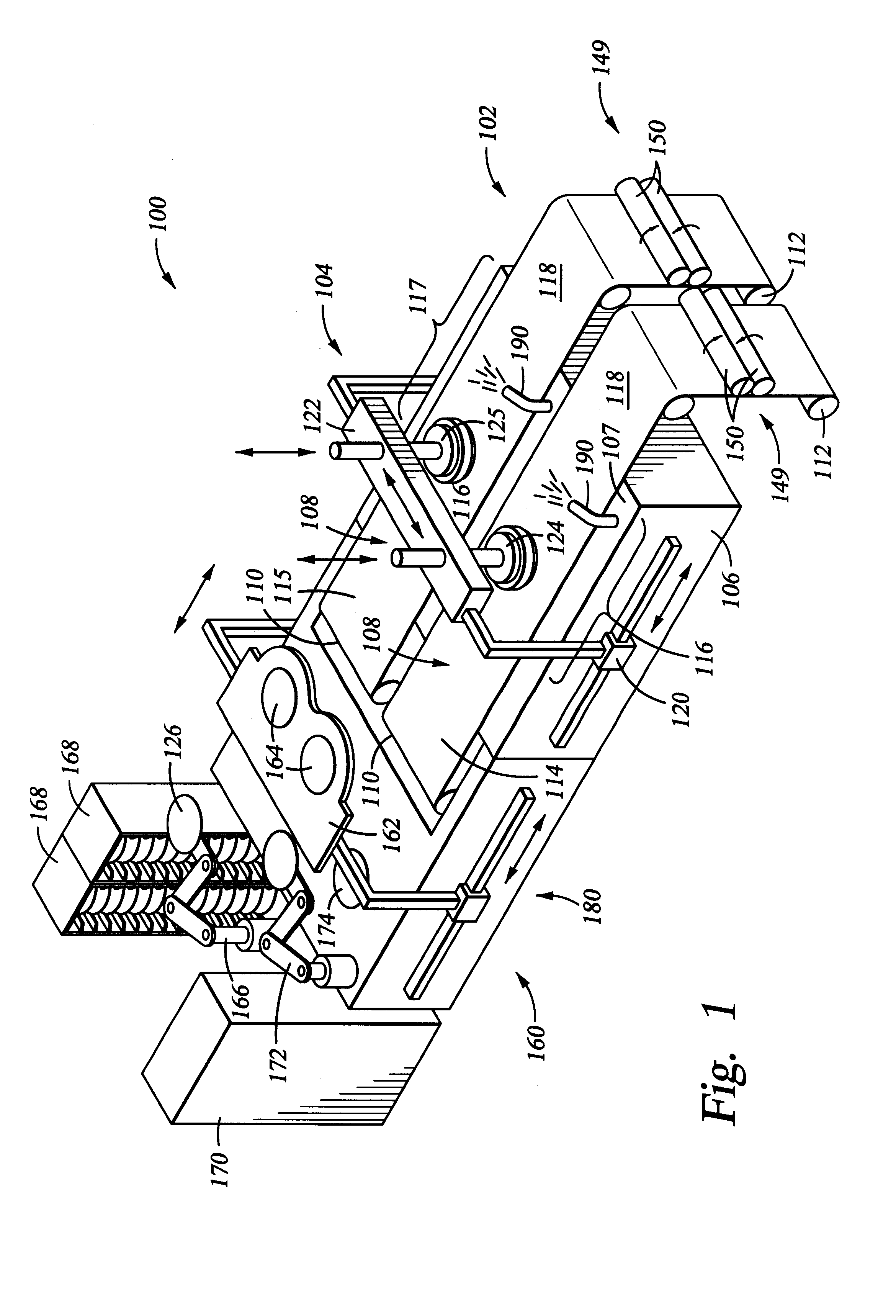
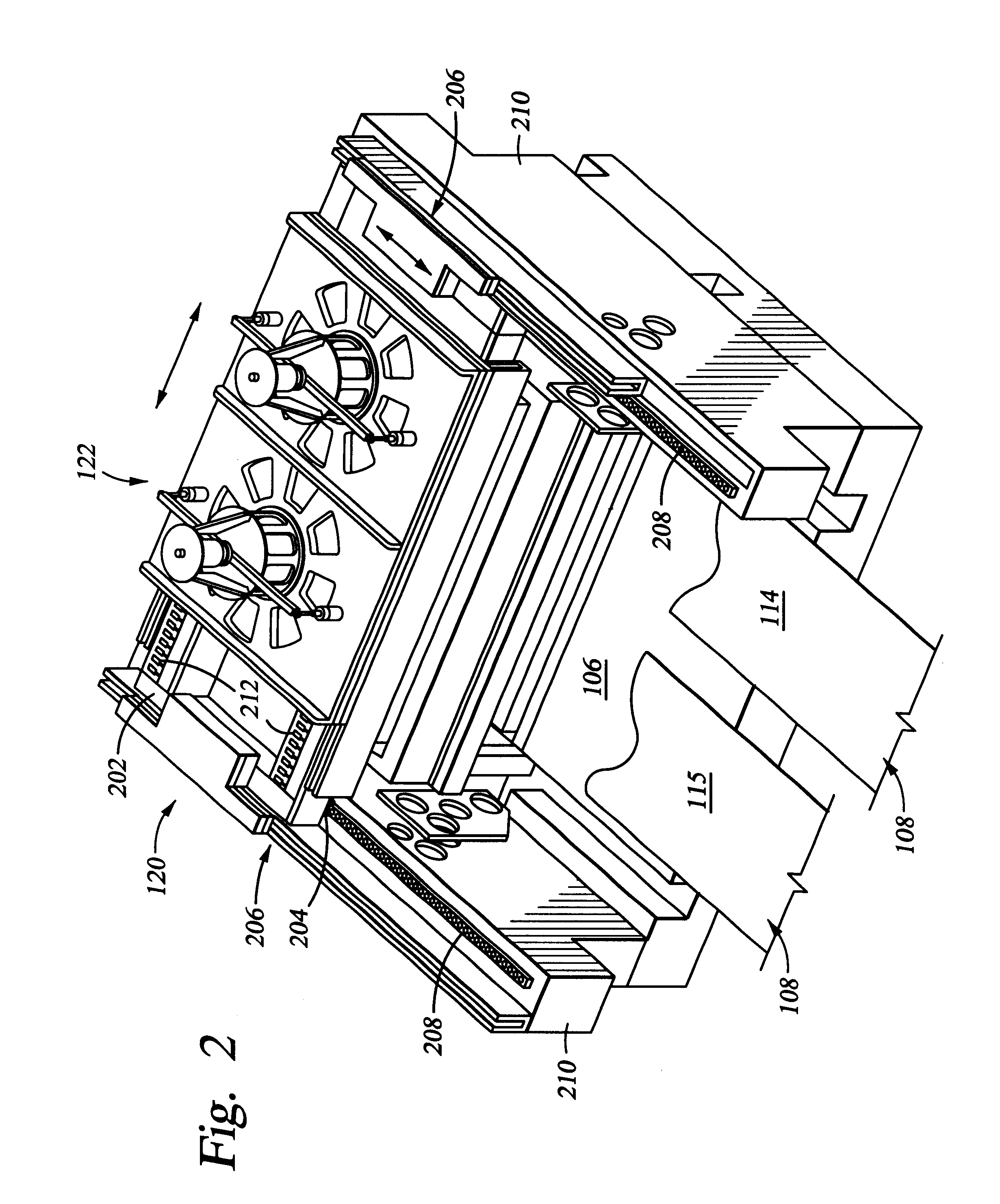
FIG. 1 depicts a schematic view of a chemical mechanical planarization system 100 including multiple conditioning webs 108a and 108b. The system 100 generally comprises a front end 160, a polishing media magazine 102, a drive system 104 and a base 106.

The front end 160 generally comprises a load station 180, a cleaner 170, and a robot 166. The robot 166 is a conventional robot 166 commonly used to transfer substrates or wafers 126 into and out of and one or more wafer cassettes 168. The typical robot 166 is a single blade robot having a vacuum gripper disposed at the end of a pair of extendable arms. By applying vacuum to the gripper, the wafer 126 is retained by the robot 166 for transfer between the cassettes 168, the load station 180, and the cleaner 170.

The load station 180 generally comprises an edge grip robot 172, one or more substrate supports 174 and a shuttle 162. Unpolished wafers 126 retrieved from the cassette 168 by the robot 166 are set on the substrate support 174. T...


PUM


Abstract

An apparatus for simultaneously polishing wafers including at least a first and a second web of polishing media. At least two polishing heads are provided on a carrier coupled to a drive system such that one polishing head positions a wafer against the first web and a second polishing head positions a second wafer against the second web. The drive system imparts a programmed polishing motion or pattern to the polishing heads.

Description

BACKGROUND OF THE DISCLOSURE1. Field of InventionThe present invention relates generally to a semiconductor wafer planarization system. More specifically, the invention relates to a planarization system having multiple polishing pads or webs.2. Background of InventionIn semiconductor wafer processing, the use of chemical mechanical planarization, or CMP, has gained favor due to the enhanced ability to stack multiple devices on a semiconductor workpiece, or substrate, such as a wafer. As the demand for planarization of layers formed on wafers in semiconductor fabrication increases, the requirement for greater system (i.e., tool) throughput with less wafer damage and enhanced wafer planarization has also increased.Two CMP systems that address these issues are described in a patent to Perlov et al. (U.S. Pat. No. 5,804,507, issued Sep. 8, 1998) and in a patent to Tolles et al. (U.S. Pat. No. 5,738,574, issued Apr. 15, 1998), both of which are hereby incorporated by reference. Perlov et...

Claims


Application Information

Patent Timeline
IPC IPC(8): B24B21/04B24B37/04B24B53/007B24B57/02B24B57/00B24B37/20B24B37/26B24B37/30B24B37/34B24B53/017
CPCB24B21/04B24B37/20B24B37/26B24B37/30B24B37/345B24B53/017B24B57/02
Inventor WHITE, JOHN M.SOMMER, PHILLIP R.FISHER, STEPHEN
Owner APPLIED MATERIALS INC
Why Eureka
Try Eureka