
Apparatus for exposing a face of a printed circuit panel

a printed circuit panel and apparatus technology, applied in the field of apparatus for exposing the face of printed circuit panels, can solve the problems of short circuit, non-uniform transformation of photosensitive materials, and shift of conductor tracks, and achieve the effects of improving the exposure of a surface, good uniformity, and good angle of inciden

Inactive Publication Date: 2003-11-11
AUTOMA TECH
View PDF1 Cites 0 Cited by
  • Summary
  • Abstract
  • Description
  • Claims
  • Application Information

AI Technical Summary

Benefits of technology

The object of the invention is to provide an exposure apparatus that makes it possible to improve exposure of a surface by scanning, in particular for manufacturing printed circuits, by providing a strip of light which presents both a good uniformity and a good angle of incidence relative to the panel.
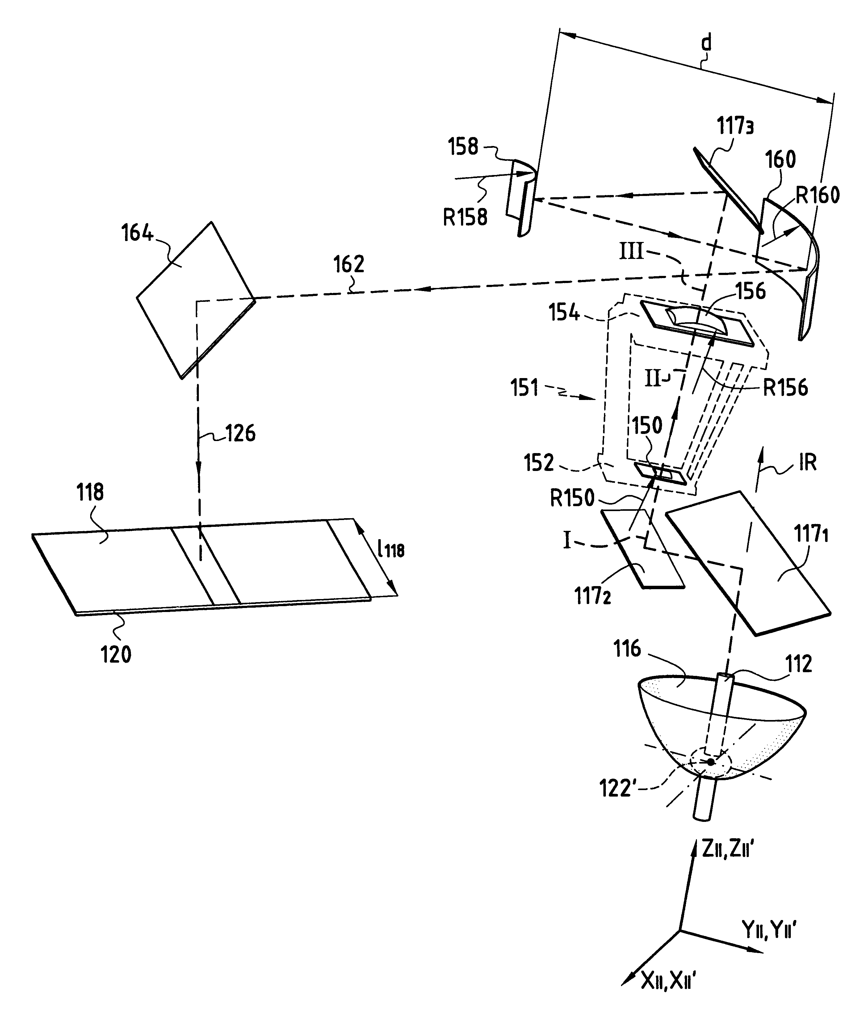
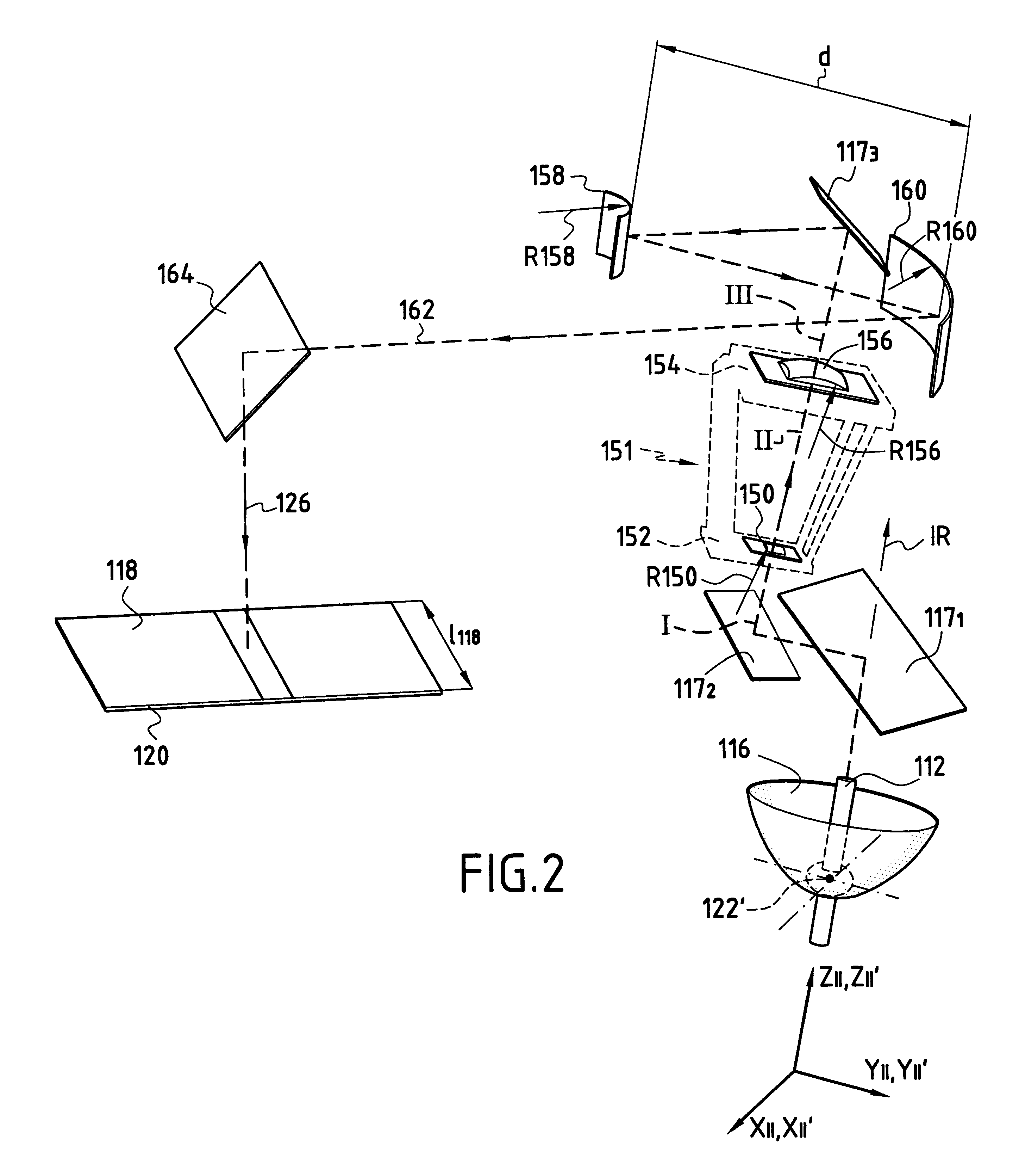
In order to obtain a light strip measuring approximately 635.times.130 mm.sup.2, the optical system advantageously comprises five light boxes in alignment along the direction extending transversely to said scanning direction, which boxes are moved in translation in the scanning direction, i.e. in a direction that is substantially transversal to the length of the light strip so as to scan the entire panel. In this optical configuration, the mean angle of incidence obtained with five medium arc lamps is about 11.degree.. Medium arc lamps make it more difficult to collimate the beam, but they make it easier to superpose the light sources.

Problems solved by technology

It will thus be understood that a light beam reaching the surface to be exposed at a poor angle of declination produces a parallax error causing the light to be offset on the surface to be exposed, thereby shifting the conductor tracks away from the design location.
Under extreme circumstances, those two phenomena taken together can lead to short circuits because tracks touch each other.
It will thus be understood that when the light beam is not uniform, it gives rise to non-uniform transformation of the photosensitive material and thus to tracks following paths that are imprecise and in extreme cases this can lead to tracks being interrupted.

Method used


Image

  • Apparatus for exposing a face of a printed circuit panel
  • Apparatus for exposing a face of a printed circuit panel
  • Apparatus for exposing a face of a printed circuit panel

Examples


Embodiment Construction

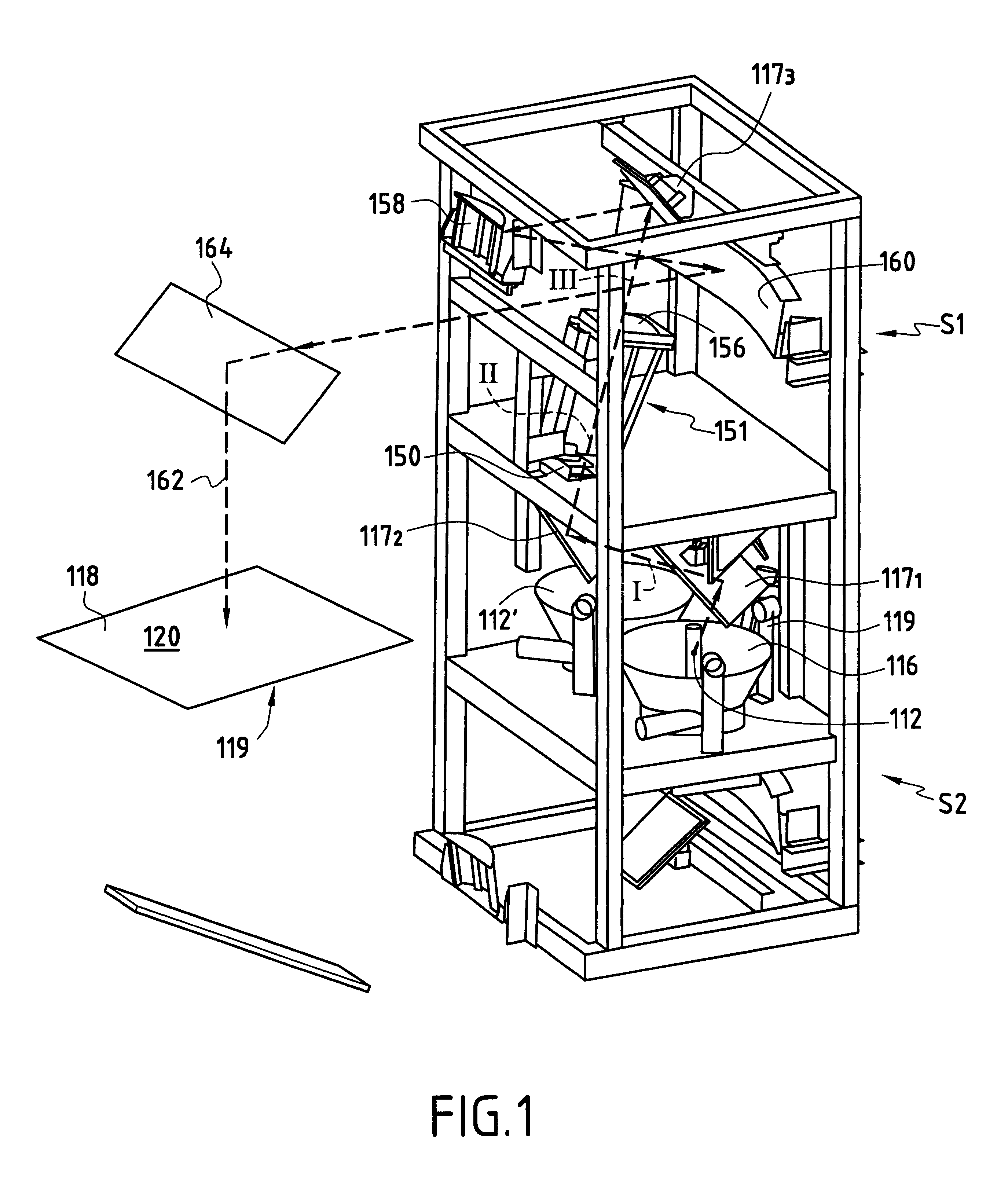
In a first aspect of the invention, the exposure apparatus for manufacturing printed circuits as shown in FIGS. 1 to 6 comprises an optical system made up of a discharge lamp and various optical elements. In this configuration, the lamp and a processor and shaper unit for acting on the light beams emitted by the lamp, and also the panel to be exposed are all stationary, and a single optical element, specifically a mirror, serves to scan the surface of the panel to be exposed.

FIG. 1 is an overall view of such apparatus together with a panel 120 to be exposed, the apparatus comprising an optical system S.sub.1 for processing and shaping a light beam emitted by a light source 112 so that it constitutes a strip. Specifically, the apparatus comprises two optical systems S.sub.1 and S.sub.2 for processing and shaping two light beams emitted by two respective light sources 112 and 112' which are placed side by side so as to expose both faces of the panel. It suffices to place two similar o...


PUM

PropertyMeasurementUnit
mean angleaaaaaaaaaa
mean angle of incidenceaaaaaaaaaa
lengthaaaaaaaaaa

Abstract

An apparatus for exposing a light sensitive surface (e.g., a printed circuit board) to light. An optical processor subsystem, which includes a reflector and an integrator-collimator assembly, processes light from a light source to produce a uniform and collimated light beam having a mean angle of incidence relative to the light sensitive surface of less than or equal to 2° and having illumination uniformity that departs by less than ±10% from a mean value. An optical light shaper subsystem transforms the uniform and collimated light beam into a uniform and collimated light strip. A displacement mechanism provides relative movement between the light strip and the light sensitive surface. A speed matching mechanism matches the speed of relative displacement to the brightness of the light strip and to the sensitivity of the light sensitive surface. The light source remains stationary in one construction and moves relative to the light sensitive panel in another construction.

Description

The present invention relates to apparatus for exposing at least one face of a panel, in particular a printed circuit panel.Such apparatuses are used for manufacturing printed circuits from a panel coated in a photosensitive material that is to have artwork placed in front of it bearing the pattern of tracks to be generated on the printed circuit. A light beam passes through the artwork and thus serves to expose the panel.Such exposure apparatuses are known, e.g. from European patents EP 618 505, EP 807 505, and EP 807 856, in which the light source and the panel to be exposed are both stationary and exposure is performed over the entire surface that is to be exposed without scanning.However, in that type of apparatus where the entire surface is exposed simultaneously, the chemical reactivity of the photosensitive material is not optimum. The efficiency of the reaction is improved when exposure is stronger and instantaneous exposure time shorter.Such apparatuses are also known in wh...

Claims


Application Information

Patent Timeline
Patent Type & Authority Patents(United States)
IPC IPC(8): G03F7/20H05K3/00
CPCG03F7/2008G03F7/201G03F7/2032G03F7/2014H05K3/0082G03F7/20
Inventor VIBET, GILLESSOREL, ALAIN
Owner AUTOMA TECH
Learn More