

Low impedance power distribution structure for a semiconductor chip package
a power distribution structure and low impedance technology, applied in semiconductor devices, semiconductor/solid-state device details, electrical equipment, etc., can solve the problems of increased susceptibility to supply line noise, increased difficulty in making low impedance power supply connections to a chip or chip, and higher impedan
- Summary
- Abstract
- Description
- Claims
- Application Information
AI Technical Summary
Benefits of technology
Problems solved by technology
Method used
Image

Examples
Embodiment Construction
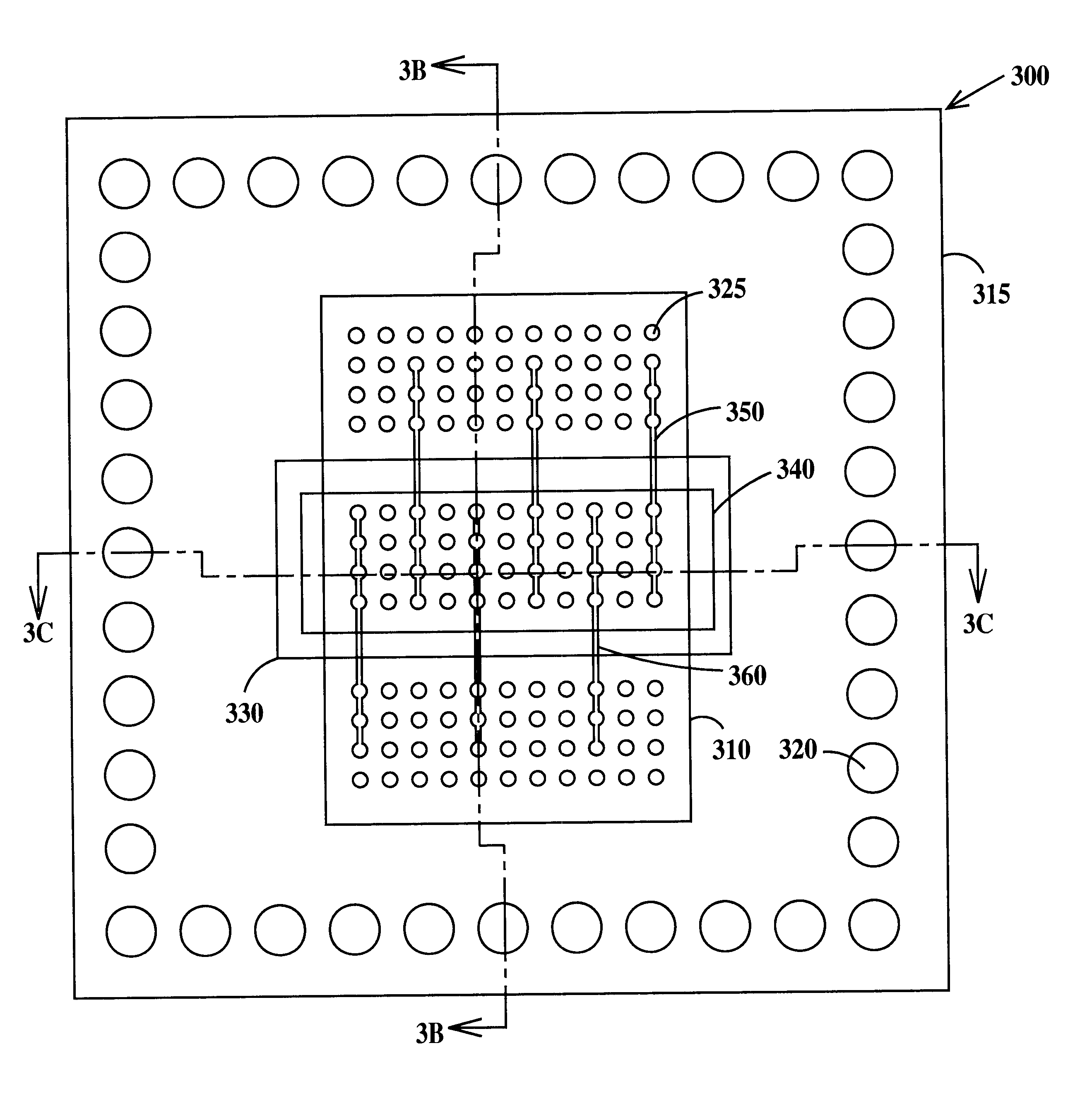
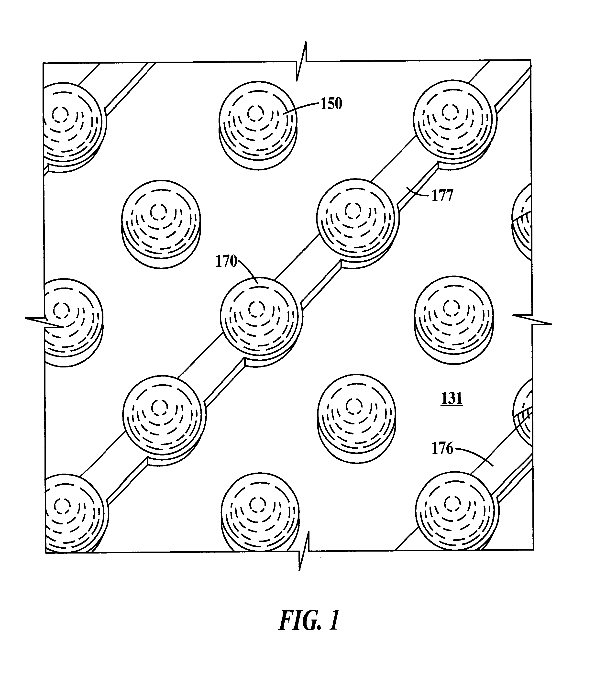
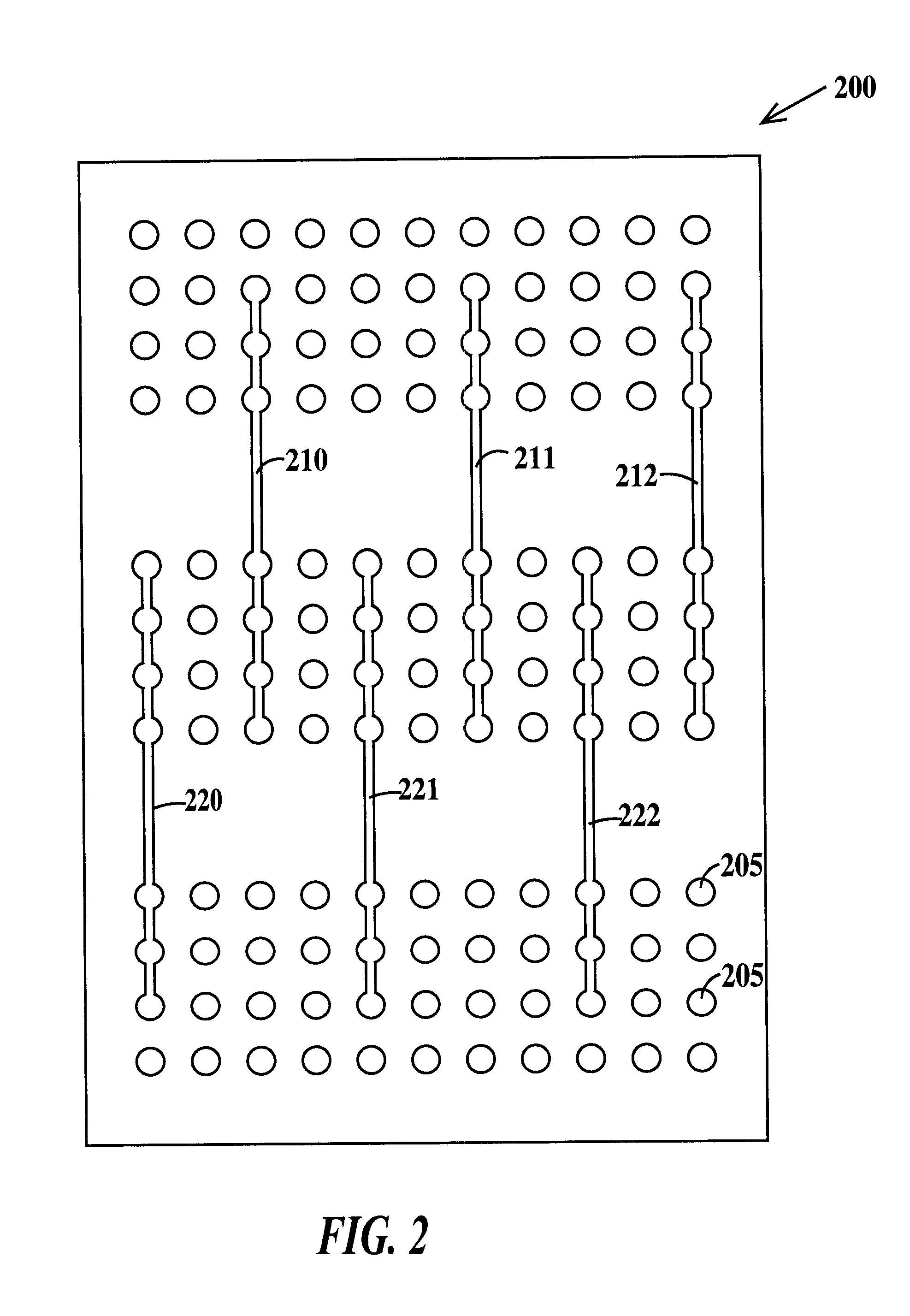
The following is a detailed explanation of the structure and method for a low impedance power distribution structure for a flip-chip type stacked chip module, and an electronic package resulting from manufacturing using embodiments of the present invention, with reference to the attached drawings. It should be noted that the same reference numbers are assigned to components having approximately the same functions and structural features in the following explanation and the attached drawings to preclude the necessity for repeated explanation thereof.
According to the present invention, a solder bump forming process is utilized to form not only solder bumps, or rounded solder balls, that make chip-to-chip connections, i.e., vertical connections, but also to use the solder bump forming process to make solder lines, i.e., electrical wires, which can provide interconnections between select solder bumps or other contact pads on the same substrate surface, i.e., horizontal connections. Thes...
PUM
 Abstract
Description
Claims
Application Information