
Method of forming alignment features for conductive devices

a technology of alignment features and conductive devices, which is applied in the direction of etching metal masks, coupling device connections, and printed element electric connection formation, etc., can solve the problems of increasing the trace density and difficulty in obtaining precise registration of mechanical alignment features with the contact portions of traces

Inactive Publication Date: 2004-03-02
ORACLE INT CORP
View PDF45 Cites 31 Cited by
  • Summary
  • Abstract
  • Description
  • Claims
  • Application Information

AI Technical Summary

Benefits of technology

Preferably, the forming steps are performed simultaneously by a photo-etching process. As a result, precise registration between the at least one mask feature and the contact portions can be achieved.

Problems solved by technology

A limiting factor for increasing the trace density is the ability to properly align the traces of one PCB with the traces of another PCB when the PCB's are electrically joined together.
Because the mechanical alignment features are formed separately from the traces, it is difficult to obtain precise registration of the mechanical alignment features with the contact portions of the traces.

Method used


Image

  • Method of forming alignment features for conductive devices
  • Method of forming alignment features for conductive devices
  • Method of forming alignment features for conductive devices

Examples


Embodiment Construction

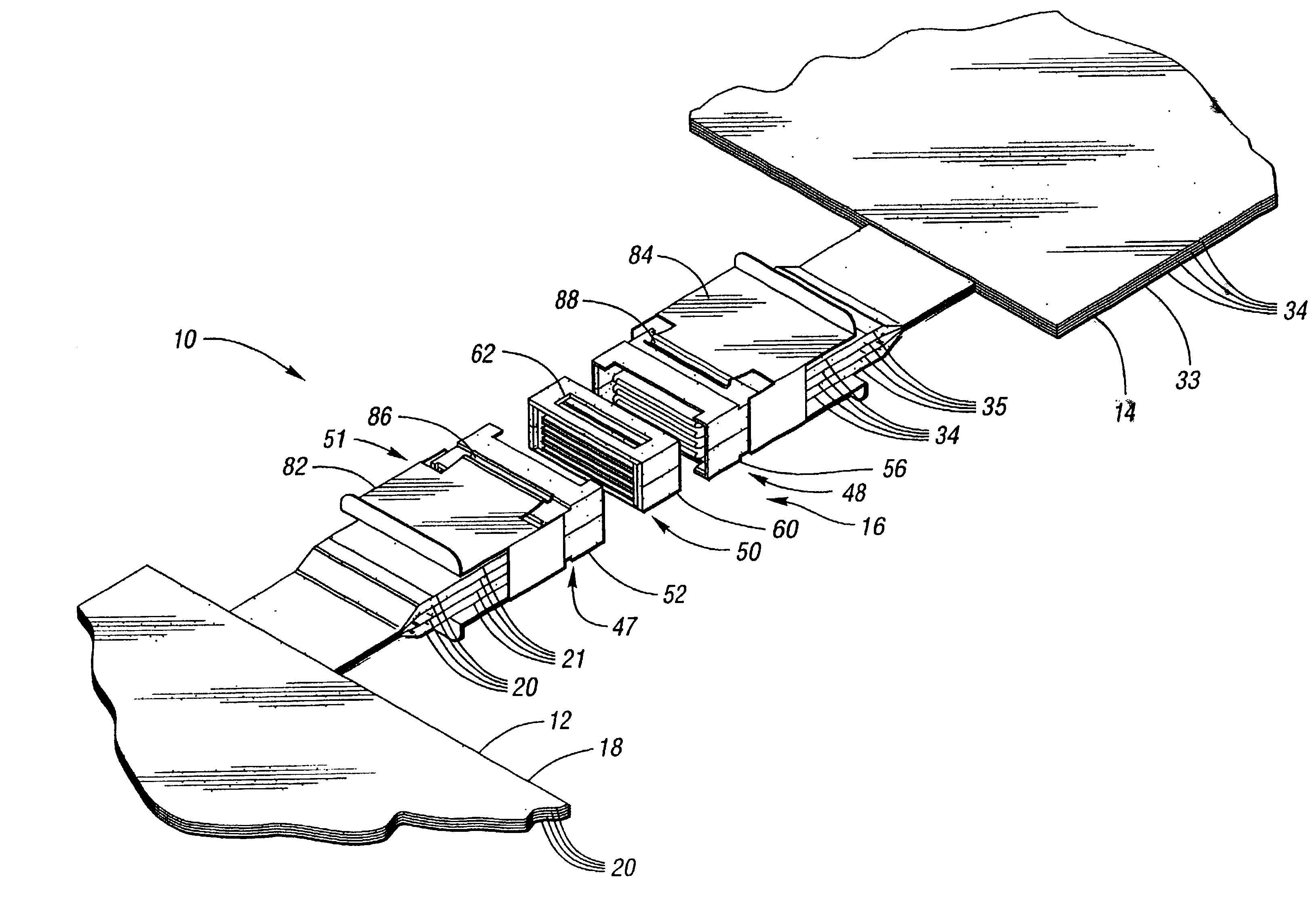
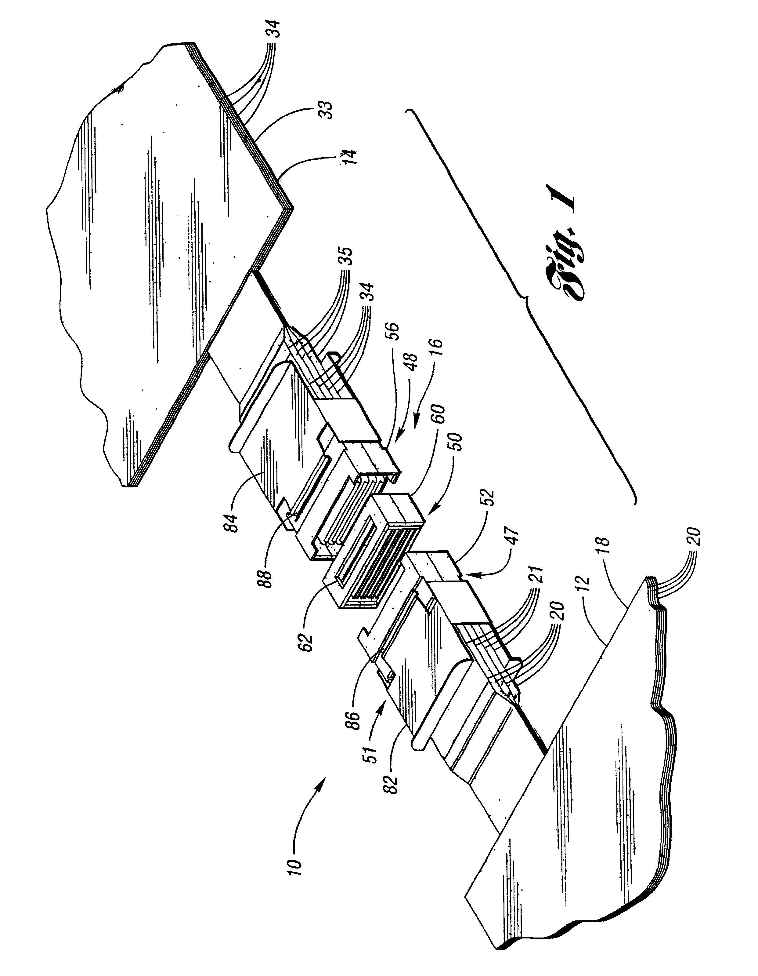
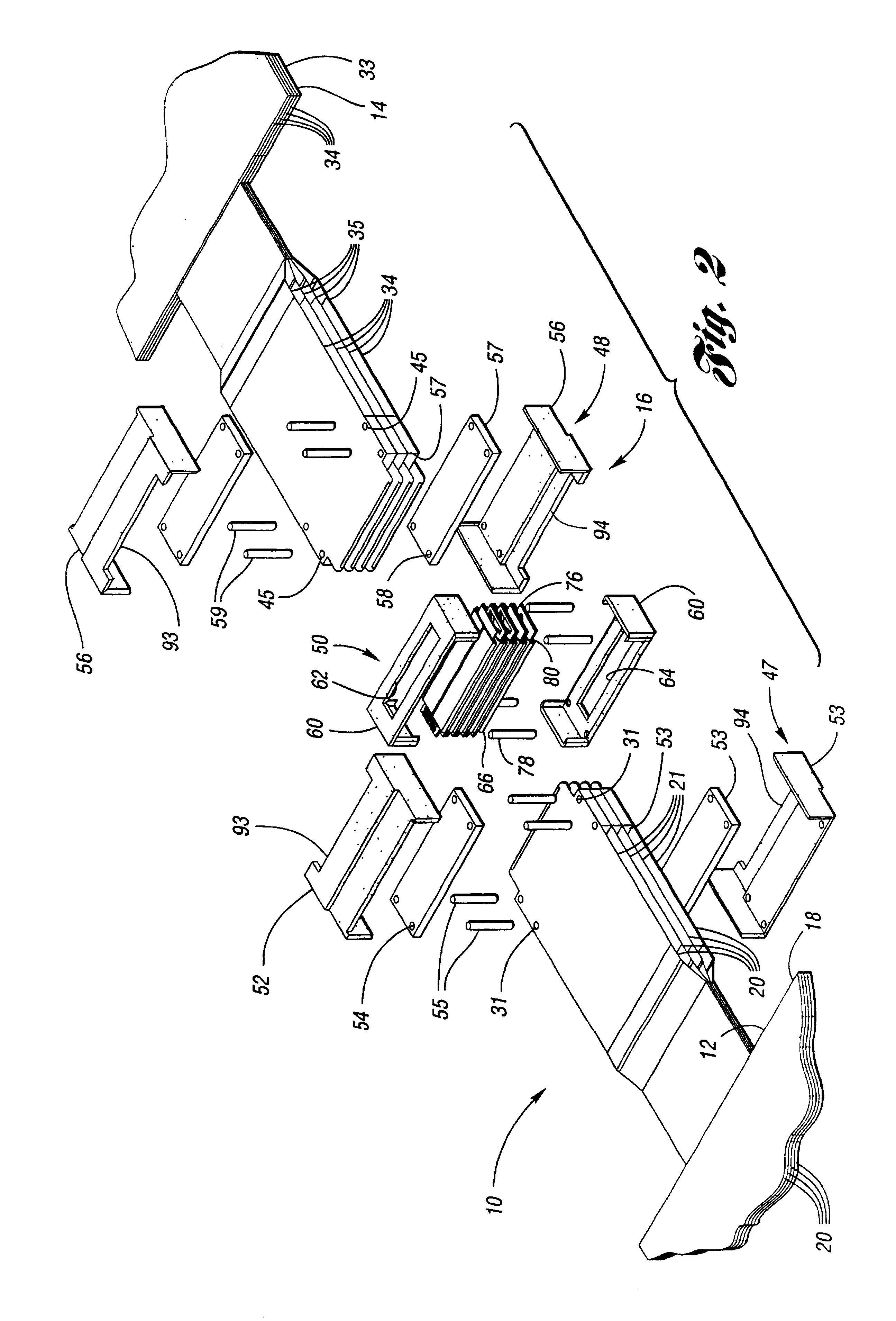
FIGS. 1-4 show a conductive system or network 10 for use in computer and / or electronic equipment, such as data processing equipment and networking equipment. The network 10 includes first and second conductive devices, such as first and second multi-layer printed circuit boards (PCB's) 12 and 14, respectively, and a connector assembly 16 for connecting together the PCB's 12 and 14. The first PCB 12 has a first main body 18 that includes multiple first signal layers 20. A portion 21 of each first signal layer 20 preferably extends beyond the first main body 18 so as to provide access to each first signal layer 20. Furthermore, the portions 21 are preferably flexible and not bonded to each other proximate distal ends of the portions 21, so that the portions 21 are independently moveable.

Referring to FIGS. 5 and 6, each first signal layer 20 has a first substrate 22, a plurality of first conductive paths or traces 24 disposed on one side of the first substrate 22, and a first ground pl...


PUM

PropertyMeasurementUnit
widthaaaaaaaaaa
radiusaaaaaaaaaa
conductiveaaaaaaaaaa

Abstract

A method of forming a conductive device includes forming a conductive layer on a substrate; etching the conductive layer to form a plurality of conductive traces; etching the conductive layer to form at least one mask feature; and removing substrate material that is not covered by the at least one mask feature so as to form at least one mechanical alignment feature.

Description

The invention relates to an improved method for forming alignment features on conductive devices.An important and continuing goal in the computer and electronics industries is that of increasing conductive or signal trace density and bandwidth of conductive devices, such as printed circuit boards (PCB's). A limiting factor for increasing the trace density is the ability to properly align the traces of one PCB with the traces of another PCB when the PCB's are electrically joined together. In order to align the traces of the PCB's, alignment features are typically formed on each PCB.A prior method of forming a PCB with such alignment features includes forming a plurality of traces on a substrate. The PCB is then inserted into a drilling device, and a drill bit of the drilling device is optically aligned with contact portions of the traces. Next, the drill bit is used to form a plurality of mechanical alignment features such as holes in the board. The holes may then be used to pin the ...

Claims


Application Information

Patent Timeline
Patent Type & Authority Patents(United States)
IPC IPC(8): H01R12/24H01R12/00H05K1/11H05K3/00H05K3/40H05K3/36
CPCH01R23/667H05K1/118H05K3/0032H05K3/365H05K3/4092Y10T29/49156H05K2201/09063H05K2203/0554H05K2203/167H01R12/85H05K2201/0397H01R12/78
Inventor SVENKESON, JOHN W.HAMRE, JOHN D.
Owner ORACLE INT CORP
Learn More